
A 3MHz Transimpedance Amplifier: Optical Speed Measurements
June 23, 2012
This note describes bandwidth measurements of a 3 MHz transimpedance photodiode amplifier using modest test equipment.
The speed performance of a photodiode amplifier can be characterized using either AC modulation techniques, or fast pulse rise and fall time characterization.
It can be shown that even for a 2nd order low-pass transfer function such as the transimpedance circuit, the f3db bandwidth and 10-90% risetime are closely approximated by:

In both these methods, an optical
source with sufficient bandwidth, ideally at least ten-times faster than the bandwidth of the circuit to be measured, is required.
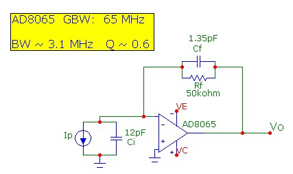
The Transimpedance Photodiode Amplifier
The transimpedance amplifier characterized here uses an AD8065 op-amp with a GBW product of 65 MHz. The Si pin photodiode is a Vishay BPW24R with a bandwidth
of ~ 50 MHz (tr ~ 7 ns). The schematic diagram below shows
the circuit, with a feedback resistance of 50kohm. A feedback capacitor of 1pF is added to ensure phase stability and remove any ringing. For a given value of Rf, which usually is
determined by the gain required in a particular application, it is easy to determine suitable values of Cf to ensure stability.
(The circuit without the 1 pF capacitor is also measured for comparison). With a stray feedback shunt capacitance estimated to be 0.35 pF, the total feedback capacitance is 1.35pF.
The total input capacitance at the inverting input (combined op-amp capacitances, photodiode capacitance of ~ 3 pF under reverse bias, and stray protoboard capacitance) is ~ 12 pF.
Circuit modelling predicts a -3dB transimpedance bandwidth of 3.1 MHz with a Q of 0.6, slightly more heavily damped
than the maximally flat case:

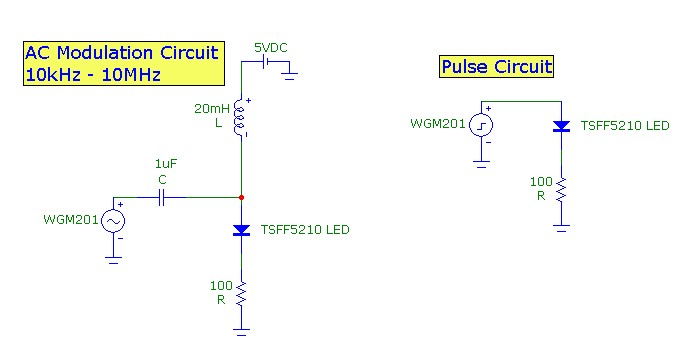
Optical Source
A 24 MHz Vishay TSFF5210 IR-LED emitting at a wavelength of 870 nm,. with rise/fall time capability of 15 ns was used for optical speed characterization. For AC modulation bandwidth measurements,
a simple bias-insertion circuit was used. The DC bias current was set at ~ 30 mA with a current modulation of ~ 15 mA. The 1 uF capacitor combined with the 100 ohm
resistor provide a flat response down to 10 kHz. The 10 mH inductor isolated the DC bias from the modulating AC voltage source above 10 kHz:

For rise-time measurements, a very simple series circuit was used with current pulse amplitude of ~ 30 mA. A square-wave drive voltage was used. With this 50% duty-cycle
drive, the TSFF5210 can in fact be driven to well over 100 mA, and up to 1A for duty cycles less than 1% for pulses ~ 10 uS or shorter.
The function generator for both pulse and sine-wave was a Syscomp Electronic Design Ltd. WGM-201 Advanced Waveform Generator with a source
resistance of 150ohm, capable of sourcing ~ 70 mA into a short circuit, 50 mA into a 50ohm load or 40 mA into 100ohms (as used in the circuits above). Pulse rise/fall
time with the WGM201 is ~ 20 ns as measured with a 1 GHz oscilloscope, comparable to the intrinsic IR-LED rise time:

Schematics of both LED drive circuits are shown below:
Optical Power and Output Voltage
Predicting optical power received and determining the corresponding photocurrent and output voltage from a transimpedance circuit is important in practical optical design.
For the transimpedance circuit, the output signal voltage in mV units (in the passband of the circuit) is related to the incident power on the photodiode active area and the photodiode responsivity by:

where Rλ is the optical-wavelength dependent photodiode Responsivity in units of A/W (or equivalently mA/mW), Rf is the transimpedance feedback resistance in ohms, and Po is the optical
power, in mW units, received by the active area of the photodiode. In more useful units of kohm for the resistance and microwatts for the optical power, the ratio of output voltage in mV to input optical power is:

For example, the specification sheet for the Vishay TSFF5210 IR-LED states the wavelength at the peak of the spectrum is 870 nm. The Vishay BPW24R Si pin photodiode shows
a responsivity at λ = 870 nm of 0.6 mA/mW. In the transimpedance circuit above, Rf = 50kohm, so the expected output voltage to input optical power ratio is 30 mV/µW
The amount of power actually received by the photodiode depends (1) the total power emitted by the LED, (2) the optical radiation pattern from the LED,
(3) the distance between the LED and the photodiode, (4) if lensing is used to assist in collecting more of the LED radiation and (5) the active area of the receiving photodiode.
For example in the AC modulation test setup, the LED was positioned at a distance L = 150 mm (6") from the photodiode. The LED was DC biased at 31 mA. According to the TSFF5210 specification,
the radiant intensity Ie of this LED at this current is 40 mW/steradian (at the peak of the forward emission pattern). On the receiver side, the BPW24R photodiode is a lensed device with a lens diameter of 4 mm
(or effective receiving area Adet of 12 mm^2).
The received optical power, in terms of radiant intensity, distance from source to photodiode and photodiode active area is given by:

where A/L^2 is the solid angle subtended by the photodiode lens relative to the LED. With the components and distance above, the received optical power is calculated to be 21 μW. With the transimpedance
circuit above, this corresponds to an output voltage of 21*30 = 630 mV. The actual measured output voltage with this setup was 800mV, in good agreement considering the uncertainty
in the specification parameters.
The scope trace below shows the output voltage from the transimpedance circuit, with the LED positioned and biased approximately as described above and modulated at 40% at 1 MHz:

Pulsed Response
The transimpedance circuit output was measured using a 2 MHz Syscomp Electronic Design Ltd. DSO-101 Digital Storage Oscilloscope.
The scope traces below show the transient response of the transimpedance circuit with Cf= 1.35 pF and Cf = 0.35 pF (with the 1pf capacitor disconnected). The fall-time
with Cf=1.35 pF is ~ 110 - 120 ns, close to the limit of this scope and consistent with a 3dB transimpedance bandwidth of 3.1 MHz with no overshoot. When the 1 pF capacitor is removed, the transimpedance
circuit becomes less damped with strong ringing with a resultant Q calculated to be ~ 1.9. The time between successive peaks can conveniently be used to determine the f3db bandwidth in this case to
be ~ 6 MHz, in agreement with frequency-domain simulation results.


Frequency Response
To determine frequency response (f3db point), the LED output, WGM-201 function generator output and the 2 MHz BW DSO-101 oscilloscope response corrections were all taken into account.
For Cf = 1.35, the f3db frequency was determined to be ~ 3.3 MHz in reasonable agreement with the simulation result of 3.1 MHz and consistent with the 10-90% transient response measurement.
With the capacitor removed (Cf = 0.35pF), the measured f3db
as 6 - 7 MHz, in agreement with the simulation results and the measured transient response.
Minimum Detectable Power
Generally, to maximize signal-to-noise performance, it is best to place as much gain (high Rf) in the transimpedance circuit as possible provided there is sufficient bandwidth available from the op-amp with the circuit components.
For a given circuit configuration (op-amp GBW, en, in, Rf, Cf, Ci) a good measure of the circuit's performance is the NEP or noise-equivalent-power. This is the received optical power which converts to an output voltage
equal to the RMS total output noise voltage. Since the noise voltage is a continuous spectral noise, the output bandwidth filtering must be considered.
The output noise voltage for the transimpedance circuit is composed of thermal noise due to Rf and amplified op-amp voltage and current noise sources.
The relative importance of each source depends on all the component values and the op-amp specifications.
These noise sources are "amplified" in different ways by the circuit. A noise calculator is available which accurately computes the output noise and its components.
For the circuit above, with Cf = 1.35pF, the f3db transimpedance bandwidth is 3.1 MHz. Assuming for simplicity that the output of the transimpedance circuit is filtered with a sharp-cutoff filter at
twice this frequency (6.2 MHz), the total output voltage noise up to 6.2 MHz is calculated to be 146μV, dominated by the op-amp voltage noise (137 μV) with some thermal noise contribution (51 μV).
Since the photodiode signal gain (see above) is 30 mV/µW or equivalently 30 µV/nW in this transimpedance circuit,
the received optical power equivalent to the output total noise voltage in a noise bandwdith of 6.2 MHz, or the NEP is 5nW.
This is the minimum detectable optical power in this circuit.