
Noise Study: How changing Cf changes the output noise:
June 30, 2012
 This study demonstrates using simulation how the output voltage noise of a typical transimpedance amplifier changes as the feedback capacitance Cf is change with all other
parameters held constant.
A typical medium speed op-amp is used and results for the common range of Q values are presented:
This study demonstrates using simulation how the output voltage noise of a typical transimpedance amplifier changes as the feedback capacitance Cf is change with all other
parameters held constant.
A typical medium speed op-amp is used and results for the common range of Q values are presented:
- Q= 0.50 (critically dampled .. excellent stability)
- Q= 0.71 (maximally flat frequency response ... very good stability)
- Q=1.00 (some peaking in frequency and pulse response ... good stability)
A typical FET input op-amp is assumed. The op-amp is modelled as ideal except for the following characteristics:
- GBW=65 MHz single-pole rolloff
- en=7 nV/√Hz
- in=1 fA/√Hz
Ri is >> Rf and is not included. Any capacitance at the non-inverting input to ground is lumped into the fixed Ci value of 12 pF. Rf is fixed at 50kΩ
The effect of changing Ri is also discussed.
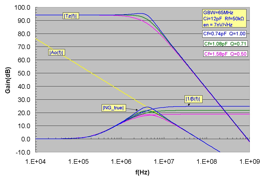
Transimpedance and Noise Gains
The graph below shows the open-loop gain, transimpedance, true noise gain and noise gain (1/beta) for the three Cf values. The true noise-gain, i.e. the complete noise gain
profile experienced by en,
becomes GREATER as we reduce Cf which tends to eliminate the noise-gain "plateau" between the noise-gain zero and noise-gain pole. Since Ci>>Cf, the noise gain
zero moves only slightly compared to the noise-gain pole:
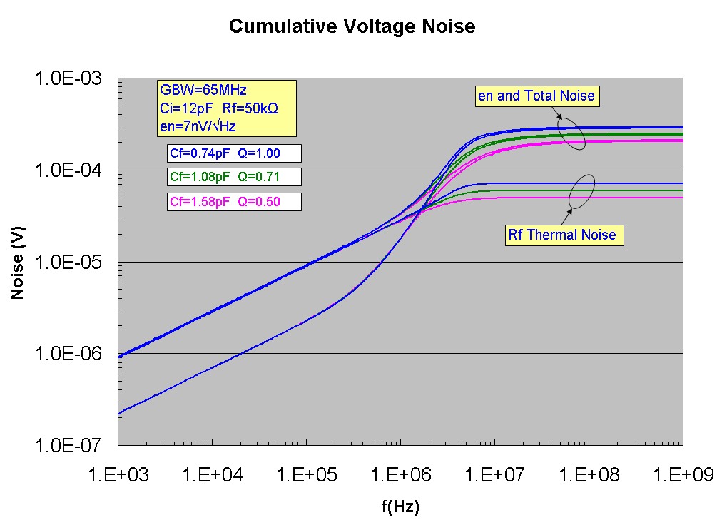
Cumulative Output Voltage Noises
The curves below show the cumulative output voltage noise (noise up to frequency f) and how they converge to the total (over all frequency) RMS noise. Note how the op-amp
voltage noise contribution "overtakes" the thermal noise contribution, a direct result of the noise-gain peaking experienced by en but not by the thermal Rf noise source.
This is also more clearly seen in the log-log plot below:

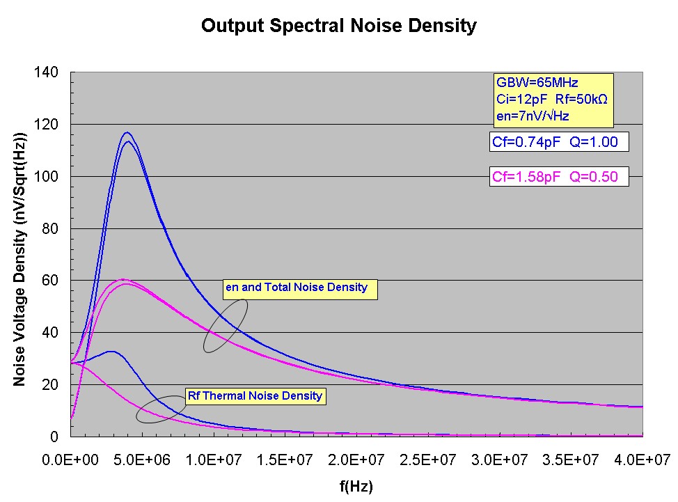
Spectral Output Voltage Noise Densities
The spectral output voltage noise-density plots (nV/√Hz) exhibit strong spectral peaking for the en noise source.
Note that even the thermal spectral noise can have some peaking effect (identical to the peaking observed in the Tz response) for higher Q values (Q=1 in this case):
Effect of Changing Ri:
In the examples above, it was assumed that Ri>>Rf which is often the case. In that scenario, the low-frequency noise gain is unity (0 dB). What happens if the net input resistance
at the inverting input is lowered, for example if the input resistance decreases significantly at high temperature? In general, the changes will depend on other circuit parameters, but for a moderate Rf value (such as 50kΩ above) and for Cf and Ci values similar
to those above, the total output voltage noise for the transimpedance circuit configuration discussed here will not change significantly, even if Ri is lowered dramatically for intermediate bandwidth cases like that discussed here. While the low frequency
DC noise gain will increase (in the example below, by 6 dB), the noise-gain zero frequency will also move to higher frequency and this will tend to in fact LOWER the range of noise-gain peaking experienced by en.
Note that the noise-gain pole frequency will not change and the asymptotic noise-gain (1/β(f)) value at high frequency will still be (Cf+Ci)/Cf independent of Ri and Rf.
The example
below shows changing the Ri value from 1GΩ to a low value of Ri = Rf (50kΩ). Comparing the plots, it is clear that most of the noise-gain contribution for en is at
higher frequency and the resultant true noise-gain curves in the main contributing spectral region are almost identical for the two Ri values. It is important to remember that typical gain plots use logarithmic
frequency scales. This means that the lower frequency noise-gain regions visually appear to make a greater contribution then is actually the case.
In the example below, the contribution to the total output voltage noise decreases slightly for the en contribution but INCREASES slightly due to the thermal noise increase (resulting from the higher DC noise gain).
The net effect as verified by an exact calculation is a slight increase in the TOTAL output voltage noise from 248 µV (for Ri=1GΩ) to 251 µV (for Ri = Rf = 50kΩ).
The second plot below shows details in the region of the noise-gain peaking:

