
How Much Cf in Transimpedance Amplifier?
Aug 05, 2012
 Transimpedance photodiode amplifier design requires special attention to stability against positive feedback in the feedback network.
Instability can arise from the zero in the noise gain (or equivalently the pole in the feedback fraction β(f)) due to the combination of the
feedback resistor Rf and the total input capacitance at the inverting input Ci which shifts the phase of the feedback signal towards positive feedback.
The solution which is often specified is to add extra feedback capacitance Cf in parallel with the feedback resistor Rf.
This introduces a pole in the noise gain (or equivalently a zero in β(f)) which compensates
the phase shift due to the zero in the noise gain. In other words, the noise gain, which starts to increase due to the zero, is flattened out by the pole phase shift.
The noise gain must be "reasonably flat" at the frequency where the noise-gain curve intersects the op-amp open-loop gain curve.
This is equivalent to saying that the phase margin at this intersection point must be sufficiently high, typically 50 degrees or higher, which guarantees good stability against oscillation.
Transimpedance photodiode amplifier design requires special attention to stability against positive feedback in the feedback network.
Instability can arise from the zero in the noise gain (or equivalently the pole in the feedback fraction β(f)) due to the combination of the
feedback resistor Rf and the total input capacitance at the inverting input Ci which shifts the phase of the feedback signal towards positive feedback.
The solution which is often specified is to add extra feedback capacitance Cf in parallel with the feedback resistor Rf.
This introduces a pole in the noise gain (or equivalently a zero in β(f)) which compensates
the phase shift due to the zero in the noise gain. In other words, the noise gain, which starts to increase due to the zero, is flattened out by the pole phase shift.
The noise gain must be "reasonably flat" at the frequency where the noise-gain curve intersects the op-amp open-loop gain curve.
This is equivalent to saying that the phase margin at this intersection point must be sufficiently high, typically 50 degrees or higher, which guarantees good stability against oscillation.
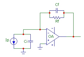
However there are two situations where it is NOT necessary to add Cf in order to ensure stability for two different reasons.
These conditions arise when the parameters Rf, Ci and GBW are such that:
- the zero frequency of the noise gain, with Cf=0, is at a higher frequency than the op-amp GBW product (or the Funity frequency)

- the capacitance Cf required to provide sufficient phase margin is so low that stray Cf (typically 0.2 pF - 0.5pF) is sufficient
The first case (discussed in greater detail below) occurs for very low values of Cf, Rf or GBW in which case the zero and pole frequencies are higher than GBW and therefore don't affect the stability significantly.
In this case the transimpedance f3db bandwidth will be comparable to, or slightly higher (due to peaking) than the op-amp GBW product.
The second case occurs for high values of Rf or GBW in which case the zero frequency is significantly LOWER than the GBW but the pole frequency is at a low enough frequency to provide the necessary compensation before the intersection point.
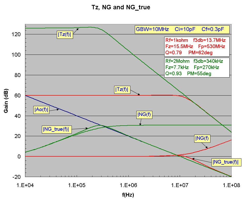
The plot below shows these two cases. The example uses a fixed GBW=10MHz and Ci=10pF with
Rf = 1kohm for the first case and Rf = 2 Mohm for the second case. A stray capacitance of Cf=0.3pF is assumed. Neither case requires additional Cf:
For comparison an intermediate case with Rf = 10kohm is shown below, demonstrating an unstable design with Cf = 0.3pF and the stabilized design with Cf = 3.0pF:

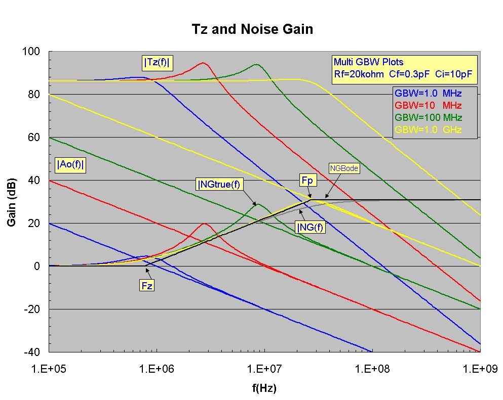
Another way of viewing the stability dependence is fixing the circuit components (Rf, Cf, Ci) and varying the op-amp GBW product.
For example the plot below displays Tz(f), noise-gain and true noise-gain with fixed circuit component values (Rf=20kohm,
Cf = 0.3pF and Ci=10pF) for different op-amp GBW values: 1MHz, 10 MHz, 100 MHz and 1 GHz.
The 1MHz and 1GHz GBW results do not require additional Cf, but the 10 and 100 MHz op-amps would require additional Cf to ensure stability.
The solid black line is the Bode approximation to the noise-gain showing the
positions of the noise-gain zero and pole: Fz (773 kHz) and Fp (26.5MHz) which are identical for the four cases:
Transimpedance Calculator:
The script calculator below determines the exact F3db transimpedance bandwidth, Q value and output noise voltages in μV for the basic transimpedance circuit. To use, enter the op-amp GBW,
and the op-amp noise spectral density values en and in. Then enter the component values for Rf, Cf and Ci
and click Get Parameters. Note the required units for each input field.
If the required Cf value is to be determined, start with a low typical stray value of 0.3pF.
If the resultant Q value is < =1.0 then the circuit will be stable with reasonably good phase margin (typically >45degrees) and no additional Cf need be added.
However, if the Q value is greater than 1, corresponding to a circuit with significant overshoot in time and peaking in frequency, then feedback stability will likely be a problem.
In that case, three special buttons are provided which assist in calculating an optimum Cf value.
These three buttons target the three common design targets for Q with Q=1 being roughly the maximum Q value which will have sufficient phase margin to produce a stable design.
The Butterworth maximally flat response design corresponds to Q = 1/√2. However, depending on the values of GBW, Rf and Ci, it may NOT be possible to achieve Q values greater than 0.5.
The overall best design targets which are stable but do not waste op-amp bandwidth have Q in the range 0.5 to 1.0.
Parameters are defined below. The noise values calculated are total noise, integrated over all frequency. (A more detailed calculator is available):
Note on Special Conditions:
Depending on the component values of Rf, Ci and GBW,
a solution for Cf
for underdamped responses, such as the maximally flat condition Q=1/√2 or the popular Q=1.0 case may not be possible.
This may occur for small values of Rf or Ci or GBW. (However, a Cf solution for the critically damped case Q = 0.5 will always be possible).
For the "maximally flat" case with Q = 1/√2, a Cf solution will only be possible under this condition:
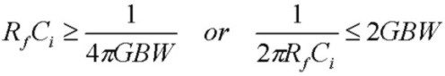
For the common case with Q = 1.0, a Cf solution will only be possible under this condition:

In both cases, this means that the zero frequency of the noise gain (or equivalently the pole frequency of the feedback factor β(f)) must be comparable to or less the op-amp GBW for a
Cf solutions with these Q values to exist. This condition will NOT be satisfied if the zero and pole frequencies of the noise-gain are considerably higher than the op-amp GBW.
In that case, the transimpedance f3db bandwidth will simply be controlled by the op-amp open-loop rolloff and f3db will be comparable to the op-amp GBW. Under this condition,
the circuit will typically have a Q value < 1.0 with Cf set to zero (or some nominally small stray value such as 0.3 pF)
and there will be negligible noise-gain peaking in the pass-band of the transimpedance response.
The circuit will have considerable phase margin and will be stable so that no compensation capacitance Cf will be required. Of course Cf could be added to reduce f3db and total
output noise.
Simply stated, if the zero frequency Fz is greater than the GBW product, the circuit will have a Q value < 1.0, will be reasonably stable and no Cf need be added.
Calculator Parameters
- GBW op-amp gain-bandwidth product
- en op-amp noise voltage spectral density
- in op-amp noise current spectral density
- Rf feedback resistance
- Cf feedback shunt capacitance
- Ci total capacitance at inverting-input to ground
- F3db 3 dB bandwidth of transimpedance transfer function
- Q quality factor of transimpedance transfer function
- F0 natural resonant frequency of transimpedance transfer function
- Ven total output noise voltage from en contribution
- Vth total output noise voltage from Rf thermal contribution
- Vin total output noise voltage from in contribution
- Vtotal total output noise voltage of all contributions (rms summed)