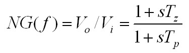
Ideal Noise-Gain
Oct 07, 2015
This note presents results for the complex noise-gain transfer function for the photodiode
transimpedance amplifier circuit such as that shown below:

The noise-gain function (along with the op-amp open loop gain profile) determines circuit stability. For transimpedance circuits,
the noise-gain is important because it determines how the op-amp input voltage noise source en is spectrally amplified by the circuit. The
noise-gain is the gain experienced by a voltage source Vi at the NONinverting terminal of the op-amp and can be easily measured this way.
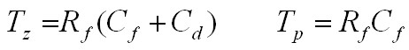
Transimpedance circuits are often characterized by fairly high photodiode capacitance Cd (compared to Cf), with the corresponding shunt
resistance Rd being much higher and is therefore ignored for simplicity in this analysis. A feedback resistance Rf and shunt capacitance Cf
,which approximately determine the transimpedance signal bandwidth, are
the other essential circuit components. Although the finite GBW product of any op-amp will affect the transfer functions (both Tz and NG) of a real circuit, and certainly
effects stability, it is useful to evaluate the ideal complex noise gain transfer function assuming a perfect op-amp with infinite GBW product.
In fact, it the intersection angle of the ideal noise-gain profile with the real op-amp open loop gain profile which directly determines stability
in these types of circuits, as discussed at the end of this article.
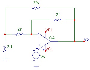
It is also interesting to study the noise-gain transfer function with a series resistance Rs added to the circuit as shown below, both outside
and inside the op-amp feedback loop which of course adds some complexity. The influence of real op-amp response and shunt resistance
on Tz(f), noise-gain and total noise is discussed in full detail elsewhere
The frequencies of the zeros fz and poles fp in terms of the corresponding characteristic "time constants" Tz and Tp are presented below where:


General Circuits
The three circuits discussed below are special cases of these very general circuits with arbitrary complex impedances Zf, Zfs, Zd and Zs
(represented as simple resistor symbols below).
The second general circuit below consists of a t-network in the feedback loop:
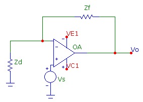


Basic Circuit
This noise gain transfer function is of first order with one zero and one pole. At high frequency, the noise-gain for this circuit
approaches a constant value of NG=(1 + Cd/Cf). If Cd>>Cf as is common in photodiode circuits, this asymptotic high-frequency noise-gain
"plateau" will be large and implies that the op-amp input noise source will continue to be amplified at frequencies well beyond
the transimpedance f-3db signal bandwidth frequency.
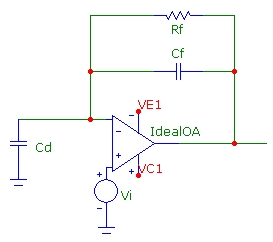
Circuit with Rs outside feedback loop

The noise gain transfer function for this circuit is of 2nd order with two real poles, and two zeros (which may be complex).

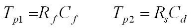
where Tp1 is the same real pole as for the basic circuit above. The additional real pole is formed by Rs and Cd.
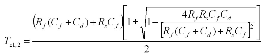
The two zeros for this circuit are:

For many cases of interest, Rf(Cf+Cd) << RsCd and the zeros are approximately:

where Tz1 is the same as for the basic circuit above and Tz2 is typically at very high frequency. Note that both the low and high frequency
noise-gain values approach unity (0 dB).
Circuit with Rs inside feedback loop

With the series resistance Rs in the feedback loop with Cd essentially in a t-network, the zeros and poles are both more complicated and both may
take on complex values indicating 2nd order resonant behaviour. The noise-gain response function is still 2nd order with two zeros and poles:
The poles are:

and the zeros are: (note they are at different frequencies than the zeros for the circuit above)
For many cases of interest, Rf(Cf+Cd) << RsCd and the zeros are approximately the same as those of the circuit above with Rs outside
the feedback loop and are typically real. However, the poles can be complex for typical values. This occurs approximately for:

Note that as for the circuit above with Rs outside the feedback loop, the low and high frequency noise-gain both approach unity (0dB).
Simulation Example
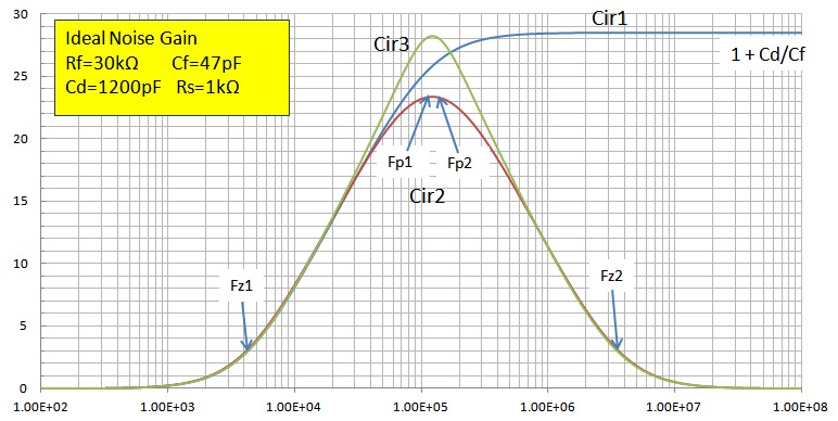
The two plots below show an example of the three circuits above for two values of Rs. The noise-gain (in db) is plotted versus log frequency.
As Rs is increased, the two poles Fp1, Fp2 for the circuits with Rs move closer together as shown.
For Rs=1000ohm, the poles for Cir3 (with Rs inside the feedback loop) are complex. The pole positions
shown are the real pole frequencies for Cir2. The resonant-like peaking behaviour for Cir3 is clearly evident.The peak noise-gain for Cir2 is reduced as the two
real poles more together and their influence overlaps resulting in attenuation of the "plateau" noise-gain:

Of course, with a real op-amp with a finite GBW product, the true high-frequency noise-gain will eventually become important and will roll-off
the noise-gain response.
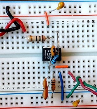
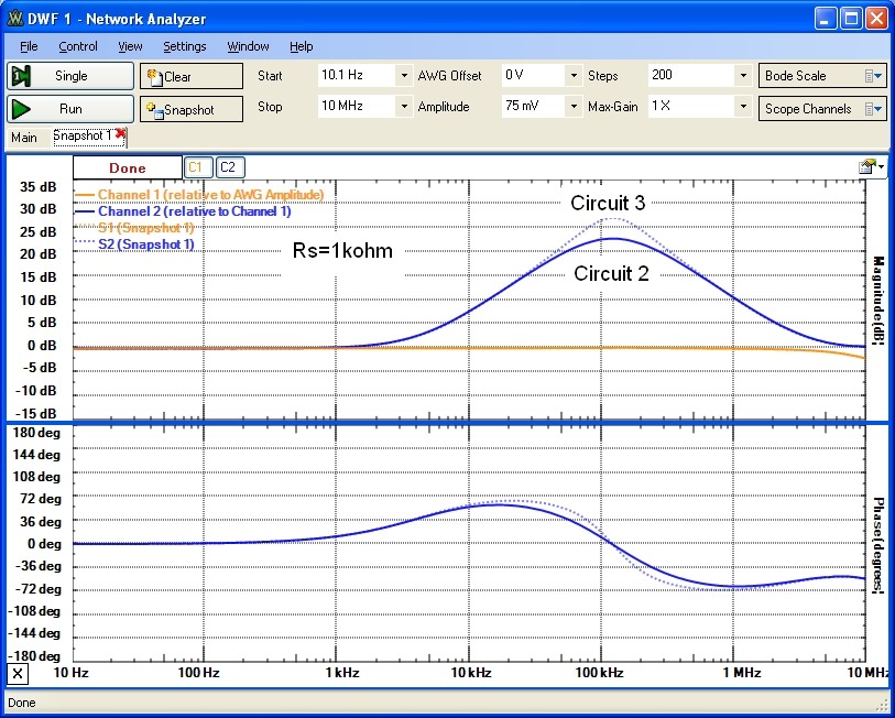
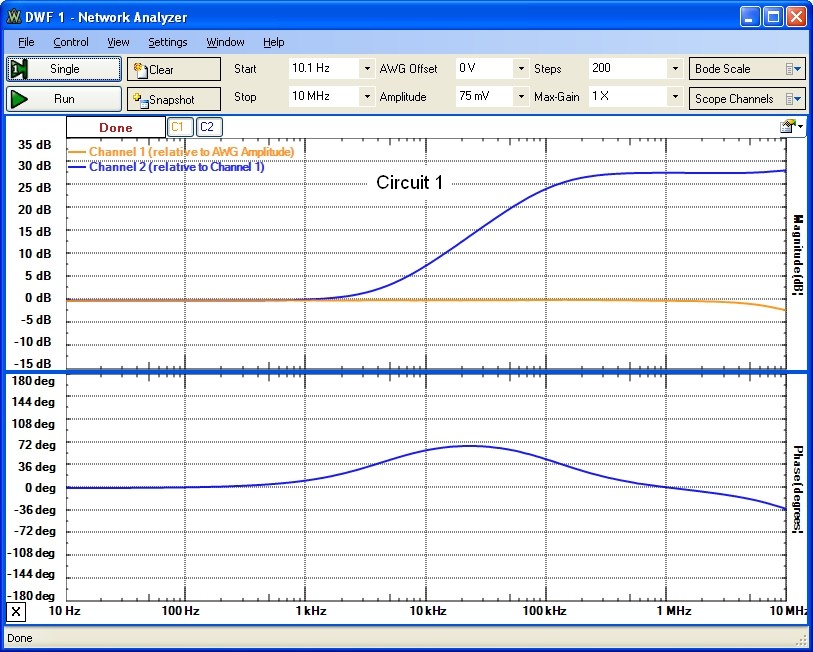
Measured Example
The Bode plots below show real noise-gain measurements on the circuits above.
A Digilent Analog Discovery
USB oscilloscope, with a useful measurement bandwidth of ~ 10MHz, was used for protoboard measurements and plotting. The voltage input level for the Bode plots was set at 75mV peak.
At the peak noise-gain level of 26.5 (28.5dB), the maximum output voltage level was ~ 2V peak.
An LT1222 op-amp with a high GBW ~ 500MHz was used to approximate
an ideal op-amp. Results are shown with circuit parameters close to those in the simulation above with Rs=0 (the basic circuit) and Rs=1000ohm (with complex poles for circuit 3).
The noise-gain profile shapes and peak amplitudes are in close agreement with the simulations above:
Effect of Op-Amp Finite GBW
The analysis, simulation and measurements above are for an ideal op-amp with infinite GBW product. This allows one to study and understand
the fundamental noise-gain shape as determined solely by the complex feedback network with a perfect virtual ground at the inverting input
of the op-amp. The measured example below shows results for the simple circuit, with Rs=0. As seen above, the IDEAL noise-gain
for this basic yet common Tz circuit has a single zero and pole with a high-frequency noise-gain plateau at (1 + Cd/Cf). The measurements below
show the influence of a finite op-amp GBW product on the true noise-gain rolloff. In this case an LT1360 (GBW=50MHz), was used and noise-gain
measurements, as above, were performed. The measured example above used an op-amp with GBW=500MHz.
The effect of the 20db/decade op-amp rolloff at high frequency is evident below.
Results are shown for Cf=12pf and Cf=47pF. For Cf=47pF, the noise-gain plateau at about 28dB (as in the "ideal" measured example above) is fairly clearly defined until the
op-amp rolloff pole becomes effective. For Cf=12pF, the noise-gain plateau , if it were reached would be ~ 40dB. In this case, the IDEAL rising noise-gain meets
the open-loop rolloff at a steep angle (corresponding to a low phase margin) corresponding to a Q value of ~ 0.8. The maximum Q value for a reasonable margin
for stability is Q ~ 1.0 which is achieved for Cf = 10pF while the Butterworth "maximally flat" Tz response, with Q=0.71 is achieved for Cf=14.2 pF.