Noise Study: Transimpedance vs Non-Inverting Amplifier
July 04, 2012
 This study compares the total output noise voltage of the transimpedance circuit and the non-inverting amplifier circuit.
The basic circuit for noise calculation purposes is shown to the right.
The comparison demonstrates how the exact expressions for the output noise voltage reduce to approximate expressions involving single-pole like noise filtering characteristics.
The different behaviour for these two circuits is a result of the different locations of the zero and pole frequencies of the noise-gain profile.
Although it is easy to calculate the exact value
of the total output voltage noise for any combination of parameters for this circuit, simplified expressions can be obtained for noise calculation in the two typical circuits
discussed here, providing greater insight into the noise performance characteristics.
This study compares the total output noise voltage of the transimpedance circuit and the non-inverting amplifier circuit.
The basic circuit for noise calculation purposes is shown to the right.
The comparison demonstrates how the exact expressions for the output noise voltage reduce to approximate expressions involving single-pole like noise filtering characteristics.
The different behaviour for these two circuits is a result of the different locations of the zero and pole frequencies of the noise-gain profile.
Although it is easy to calculate the exact value
of the total output voltage noise for any combination of parameters for this circuit, simplified expressions can be obtained for noise calculation in the two typical circuits
discussed here, providing greater insight into the noise performance characteristics.
General Exact Result
The exact expression for the total output voltage noise, summed over all frequencies, for the circuit shown above is:

where en and in are the op-amp spectral voltage and current noise densities, N0 is the DC noise gain, Kb is Boltzmann's constant, T is the absolute
temperature and Rf is the feedback resistance.
NBWen is the noise bandwidth for the voltage noise contribution, and NBWth_in is the
noise bandwidth for the current noise and resistors thermal noise contributions:


For this feedback network consisting of Ri, Ci, Rf, Cf, the zero and pole frequencies of the noise gain (1/β) are:


These expressions are exact and valid for any location of the zero and pole frequencies and for any op-amp GBW product.
The spectral noise densities will be assumed constant over frequency. Therefore 1/f noise, which will be important in low frequency circuits, is not considered. Also, the op-amp current noise
in the example below is extremely low and will be insignificant compared to the en and thermal noise contributions.
Example Comparison
The two circuits to be compared are shown below. The op-amp has GBW=65MHz with spectral noise densities as shown:

In the circuits, R and C values are the TOTAL values.
Both circuits have the same Rf of 50kohm. Ri for the non-inverting circuit is 1 Gohm a typical very high value for a FET-input op-amp. Ri for the non-inverting amplifier is 500ohm which
provides a circuit gain of 101 or ~ 40dB.
The Ci value is the total input capacitance at the inverting input to ground. For the transimpedance circuit, the value is 12 pF which would include
the op-amp capacitances and the current source (e.g. a photodiode) capacitance plus strays. The transimpedance feedback shunt capacitance Cf of 1.35pF is higher than the non-inverting input value 0f 0.4 pF (strays only).
This would correspond to adding an additional shunt capacitance for stability and phase compensation for this particular circuit.
The graph below shows the various gain plots of both circuits. The usual noise gain profile (1/β where β is the complex feedback fraction) is shown as well as the true noise gain profile which includes the
op-amp gain-bandwidth rolloff. The true noise-gain is exactly the gain profile of a non-inverting amplifier with the same circuit.

(a) Transimpedance Circuit
The component values for this circuit correspond to a typical good stability design point of Q = 0.6 with a transimpedance signal bandwidth of 3.1 MHz. The pole and zero frequencies of
the noise gain are Fp=2.4MHz and Fz=240kHz as marked on the graph above. Note that Fz is lower than Fp. This leads to significant "gain peaking" in the noise gain profile, a common
characteristic of transimpedance circuits.
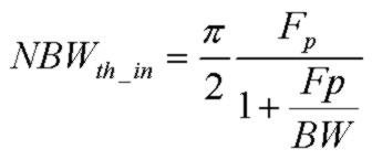
Since Ri>>Rf, the DC noise gain N0 ~ 1 so BW=GBW. Since Fp<<BW and Fz<<BW, the noise bandwidths can be approximated by:
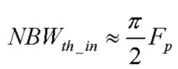

These expressions are very similar to the single-pole noise-bandwidth result for the common RC filter of π/2*f3db. For the thermal and in noise-bandwidth, the pole Frequency Fp is
the determining frequency. For the en voltage noise, the effect of the increasing noise-gain profile between Fz and Fp translates into an increased effective noise-bandwidth frequency of π/2*(Cf+Ci)/Cf*GBW.
With reference to the noise-gain curve above for the transimpedance amplifier, the ratio (Cf+Ci)/Cf is simply the asymptotic value at high-frequency of the noise gain (1/β) curve. Using this gain and
the corresponding intersection frequency with the open loop gain, Fc, the noise-bandwith for en can be rewritten:


This final expression shows that for the total output voltage noise contribution from en, the actual noise-gain amplification curve is equivalent to a noise-gain curve with a constant
and uniform gain value NG∞ with a single-pole noise bandwidth of π/2*Fc. Alternatively, the total output voltage noise from en is equivalent to a noise-gain curve with UNITY NOISE GAIN
with a very high single-pole noise bandwidth of π/2*(Cf+Ci)/Cf*GBW.
It is not difficult to show that with Ri included and as above assuming Fp<<BW and Fz<<BW, the noise bandwidth for en becomes approximately:
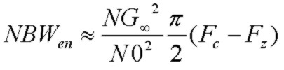
and the output voltage noise contribution from en becomes:

Again, this final expression shows that for the purposes of calculating the total output voltage noise contribution from en, the actual plateau-shaped noise-gain amplification curve
is equivalent to a simpler noise-gain curve with a constant and uniform gain value NG∞ up to a single-pole noise bandwidth of π/2*(Fc-Fz).
The Fz term also provides a more accurate correction term than the first approximate expression above.
Notice that there is only a weak dependence on Ri through the Fz term of the total output voltage noise due to en. The output voltage noise from en drops slightly as
Ri is lowered.
The plot below shows the exact output spectral voltage noise density for en and the equivalent single-pole-like spectral noise density with cutoff frequencies Fc for approx1 and (Fc-Fz)
for the more accurate approx2. These equivalent spectral densities produce (almost exactly) the same total integrated output en voltage noise as the exact curve.
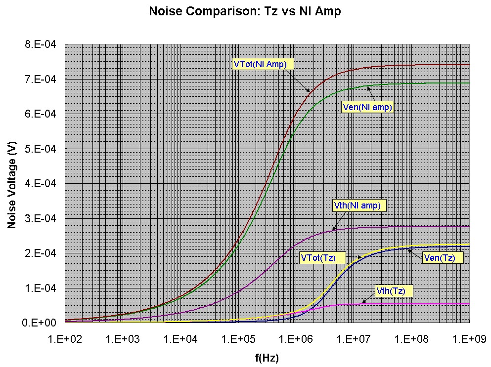
To demonstrate how the noise at higher frequencies actually dominates the total, the
plot is displayed in linear-linear form. The total en noise voltage is simply the square root of the spectral-noise (squared) area under the graph :
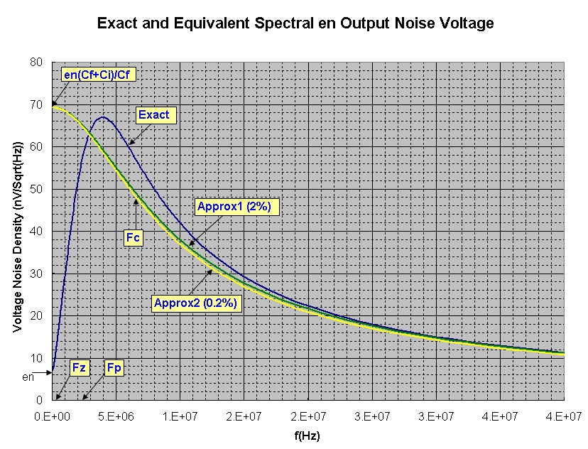
The approximate and exact results for the resultant voltage output noises for the transimpedance circuit above are:
- en voltage noise: 222.4 μV (approx) 218.4 μV (approx with Fz term) 218.9 μV(exact)
- Rf thermal noise: 54.5 μV (approx) 53.5 μV (exact)
so the approximate expressions are very close, within 2% of the exact results for the simplest approximations in this example. The more accurate approximation for the en contribution is within
0.2% of the exact result. For Ri comparable to Rf, the simplest approximation results in ~ 3-5% accuracy, while the more accurate approximation for en results in ~ 1% accuracy.
(b) Non-Inverting Amplifier Circuit
The non-inverting amplifier, a standard op-amp voltage amplifier circuit, has Ri=500ohm. With Rf=50k, this translates into a DC noise (and signal) gain of N0= 101 (40.1dB).
With reference to the plots above, it is seen that the shape of the noise-gain (1/β) curve is different than that of the transimpedance circuit. This is because the lowering of Ri
causes both Fp and Fz to increase in frequency.
The pole and zero frequencies of the noise gain are Fp=8.0MHz and Fz=50MHz as marked on the graph above.
In fact the order of Fz and Fp changes with Fz being at a higher frequency. This causes the phase and amplitude character of the noise-gain to change
as shown which improves the phase stability scenario. Also, Fz and Fp are at higher frequencies than the intersection frequency of N0 and the open-loop response, BW=GBW/N0 = 643.6kHz.
BW is approximately the f3db bandwidth of this non-inverting amplifier. (Fp slightly lowers the true f3db bandwidth to 602 kHz).
Since Fp>>BW and Fz>>BW, the noise bandwidth both can be approximated by the same simple familiar expression:
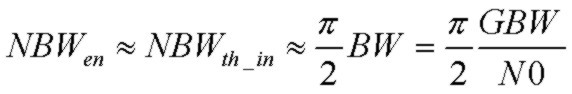
The noise bandwidth in this case is simply that of a single-pole rolloff, as seen in the graph above, at approximately the non-inverting amplifier's f3db frequency, exactly as expected.
Since Fz and Fp are at higher frequencies, the op-amps gain bandwidth limitation determines the circuit bandwidth and also the noise-bandwidth. Of course, Cf could be increased to lower
Fp which eventually would lead to narrower circuit bandwidth and a lower noise-bandwidth, controlled by the location of Fp.
The approximate and exact results for the resultant voltage output noises are:
- en voltage noise: 711 μV (approximate) 688 μV(exact)
- Rf thermal noise: 286 μV (approximate) 275 μV (exact)
so the approximate expressions are close, within 5% of the exact results.
How High is Infinite Frequency?
Since the noise results above are total noise integrated over ALL frequency, in practice how high a frequency does this mean? The cumulative output voltage noise
plots below for the transimpedance and non-inverting amplifier examples above offer some perspective and show how the cumulative output voltage noise converges to the total output voltage noise.
For the transimpedance circuit, about 90% of the total (all frequency) noise
is reached at a frequency of 20MHz, or 6X the transimpedance 3db bandwidth. This slow convergence to total noise is due to the gain peaking in the noise-gain profile. Notice
how at ~ 1.8MHz, the en cumulative noise overtakes the cumulative Rf thermal noise, a result of the strong gain peaking.
For the non-inverting amplifier, 90% of the total (all frequency) noise is reached at a frequency of 2 MHz or 3Xf3db = 3XGBW/N0. Both the en and thermal noise (of Rf and Ri) increase
at the same rate and there is no gain peaking effect: