
Elementary Transimpedance Photodiode Amplifier Design
Aug 27, 2012
The purpose of this article is to describe a simple design approach for a phododiode amplifier using the transimpedance circuit. The intent is to provide a simplified approach without explaining
the equations used. The reader is assumed familiar with basic op-amp circuits.
For complete details and discussion on the full equations and more complex designs, examples and measurements on real circuits, see Transimpedance Amplifiers .
The Basic Transimpedance Circuit:
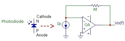
The simplest possible photodiode transimpedance amplifier circuit is shown below. It is a current to voltage converter. The photodiode is represented as an ideal current source Ip which has infinite
impedance. The photocurrent is a reverse current which under any significant load would tend to forward bias the photodiode. However, the transimpedance amplifier configuration presents
a "virtual ground" to the photodiode providing effectively an extremely small load to the photodiode which minimizes any forward bias developed across the photodiode terminals caused by photocurrent. This is achieved through the active
feedback network of Rf. The orientation of the photodiode P and N terminals are shown for
the corresponding direction of the current source Ip. In this orientation, the output voltage of the op-amp will be positive with photocurrent flowing from the op-amp output through Rf and through the photodiode.
[Note that since the photocurrent is always a reverse current, an AC frequency response implies a DC optical illumination level with a superimposed AC optical modulation. However the AC modulation level need not be
a "small signal" level].
The transimpedance is defined as the frequency-dependent ratio of output voltage to the current source or Vo(f)/Ip. The feedback network consists of a single gain-determining resistance Rf. In this very simplified model, the feedback fraction is 100% (or equivalently the noise gain is unity)
and the transimpedance 3db bandwidth is simply the unity-gain frequency of the op-amp or the op-amp GBW product. The frequency response is flat from DC to
the 3db bandwidth frequency and rolls-off beyond that point at a rate of 20 dB/decade. This elementary model is useful for very low frequency considerations:
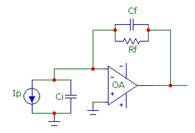
However, real transimpedance circuits are more complicated due to the capacitance Ci between the op-amp inverting input and ground. A more realistic and useful model
for a transimpedance photodiode amplifier is shown below.
Ci is the total capacitance at the inverting input, including the op-amp capacitances (typically between 5 pF and 15 pF), photodiode capacitance (varies widely, depending
mainly on the size of the photodiode and if any reverse bias is applied, between 1pF and 1000pF) and any stray circuit capacitances (typically between 0.5 - 2 pF).
As the frequency increases, this capacitance shunts the feedback signal more. This means that the feedback signal will be less than 100% (or the noise gain will be greater than unity) and it will depend on frequency.
Rf in combination with the input capacitance Ci therefore forms a complex voltage divider in the feedback network and this will lower the transimpedance bandwidth.
Furthermore, the input capacitance Ci introduces a phase shift in the feedback-signal which tends to move the circuit towards an unstable condition of positive feedback. To stabilize against instability and
potential oscillation problems, a shunt capacitance Cf is usually required. Cf is the total feedback capacitance across the feedback resistor and includes stray capacitance (typically 0.3 - 1pF) and any capacitance added to ensure circuit stability.
Generally lower Ci results in improved performance:
For simplicity, the circuit above does not show the components needed to reverse bias the photodiode, if necessary, which is often used to reduce input capacitance Ci and improve speed and lower noise.
A typical simple "bias insertion" method isolates the power supply from the transimpedance circuit.
Also, it is assumed that the total input resistance at the inverting input to ground is very high and can be ignored.
For very large area photodiodes, the Ri contribution from the
photodiode will become important. References listed above discuss its inclusion.
How Much Bandwidth?
Probably the most basic design parameter is bandwidth (speed). We will assume that frequencies from DC up to some maximum frequency F3db must be handled by the circuit.
We will assume that the photodiode is intrinsically fast enough that it only affects overall circuit bandwidth through its capacitance which is lumped into Ci.
In many cases, the best overall compromise between circuit bandwidth and circuit stability is the "Butterworth" maximally flat frequency response design with the two basic design equations:
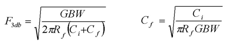
This is the value of F3db provided that the Cf value is chosen by the design equation.
The value of Cf determines circuit stability and depends on GBW, Rf and Ci. The equation for Cf is approximate and assumes that Cf<Ci which is usually true.
Furthermore, under certain conditions (very low Rf, Ci or GBW) it may not be possible to achieve the "maximally flat" response condition (see Note On Special Conditions below).
In any case, a calculator provided below can be used for any combination of circuit parameters and displays the exact results and can be used to determine the amount (if any)
of Cf required to obtain a stable circuit.
Another way of viewing bandwidth is asking what must the GBW product of the op-amp be, given Rf and Ci, to attain a required transimpedance f3db? Assuming as is often the case
that Ci>>Cf, the equation above for F3db, for the maximally flat response case, can be inverted and written as:
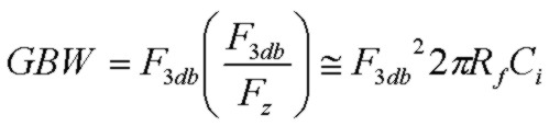
where Fz is the zero frequency 1/(2πRfCi). It is seen that:
- with fixed Rf and Ci, the required op-amp GBW product increases as the square of the target F3db
- for a required F3db, the required op-amp GBW product increases linearly with Rf and with Ci
Designing:
A common design approach starts with a requirement for a certain voltage output level from the transimpedance circuit in the pass-band.
Assume we have a specific op-amp with GBW and capacitance, and a photodiode with known capacitance:
(1) Assuming that the incident optical power Pin on the photodiode is known, the photocurrent Ip
and thus the output voltage Vout can be determined from the photodiode responsivity Resp(λ) specification:

The required output voltage level will therefore determine the required feedback resistance Rf, that is the transimpedance gain.
(Although the photodiode responsivity is optical-wavelength dependent, for basic design work an approximate responsivity of 0.5A/W can be used, a typical value for Si photodiodes in the visible region.)
(2) Using this Rf value and GBW and Ci, calculate the Cf value from the design equation above. Alternatively, use the calculator provided below.
(3) Calculate the F3db circuit bandwidth using the design equation above (or calculator below) to determine if there is sufficient bandwidth with the gain (Rf) requirements.
(4) If the circuit bandwidth is too low, explore alternate results using other GBW or Ci. If the circuit bandwidth is much higher than needed, consider using an op-amp with lower GBW or
increase Cf to force a lower bandwidth (which won't however be a "maximally flat" design). From noise considerations, an op-amp with just sufficient bandwidth is the best choice.
A calculator below assists with rapid design variations.
Collect More Light:
The typical design scenario above was based on a known optical power Pin received by the photodiode. For low-level applications, it is always best to maximize Pin by collecting as much incident optical power as possible,
through simple lensing for example. This "optical gain" is essentially noise free. For photodiode receivers using fairly monochromatic LED sources, simple lenses are perfectly adequate.
Noise:
The noise voltage at the output of the transimpedance amplifier often tends to be dominated by the contribution from the op-amp noise voltage which experiences noise gain peaking, an effect that is characteristic of transimpedance circuits.
The total output voltage noise consists of the op-amp voltage noise en, noise from the op-amp current noise in flowing through Rf and thermal noise from Rf.
The total output voltage noise will limit the minimum detectable optical signal power. The calculator below accurately computes the output noise contributions from each component and the RMS total
integrated noise voltage over the full circuit bandwidth.
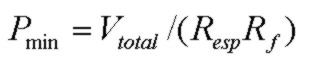
With Vtotal being the total output noise voltage, the minimum detectable optical signal power is:
and the signal-to-noise ratio for a given received optical power Pin is:

Transimpedance Calculator:
The script calculator below determines the exact F3db transimpedance bandwidth, Q value and output noise voltages in μV for the basic transimpedance circuit. To use, enter the op-amp GBW,
and the op-amp noise spectral density values en and in. Then enter the component values for Rf, Cf and Ci
and click Get Parameters. Note the required units for each input field.
If the required Cf value is to be determined, start with a low typical stray value of 0.3pF.
If the resultant Q value is < =1.0 then the circuit will be stable with reasonably good phase margin (typically >45degrees) and no additional Cf need be added.
However, if the Q value is greater than 1, corresponding to a circuit with significant overshoot in time and peaking in frequency, then feedback stability will likely be a problem.
In that case, three special buttons are provided which assist in calculating an optimum Cf value.
These three buttons target the three common design targets for Q with Q=1 being roughly the maximum Q value which will have sufficient phase margin to produce a stable design.
The Butterworth maximally flat response design corresponds to Q = 1/√2. However, depending on the values of GBW, Rf and Ci, it may NOT be possible to achieve Q values greater than 0.5.
The overall best design targets which are stable but do not waste op-amp bandwidth have Q in the range 0.5 to 1.0.
Parameters are defined below. The noise values calculated are total noise, integrated over all frequency.
(A more detailed calculator is available):
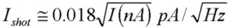
The calculator above does not include shot noise from the photodiode dark current (if reverse biased) or shot noise from the signal photocurrent. The shot noise spectral
current density in A/√(Hz) for photo or dark current I is given by:

which in convenient units is:
 or
or 
These shot noise contributions experience exactly the same transimpedance transfer function gain as the op-amp noise current density in above. The equations
can be used to quickly determine if these photodiode shot noise contributions are significant.
Note on Special Conditions:
Depending on the component values of Rf, Ci and GBW,
a solution for Cf
for underdamped responses, such as the maximally flat condition Q=1/√2 or the popular Q=1.0 case may not be possible.
This may occur for small values of Rf or Ci or GBW. (However, a Cf solution for the critically damped case Q = 0.5 will always be possible).
For the "maximally flat" case with Q = 1/√2, a Cf solution will only be possible under this condition:

For the common case with Q = 1.0, a Cf solution will only be possible under this condition:

In both cases, this means that the zero frequency of the noise gain (or equivalently the pole frequency of the feedback factor β(f)) must be comparable to or less the op-amp GBW for a
Cf solutions with these Q values to exist. This condition will NOT be satisfied if the zero and pole frequencies of the noise-gain are considerably higher than the op-amp GBW.
In that case, the transimpedance F3db bandwidth will simply be controlled by the op-amp open-loop rolloff and F3db will be comparable to the op-amp GBW. Under this condition,
the circuit will typically have a Q value < 0.5 with Cf set to zero (or some nominally small stray value such as 0.3 pF)
and there will be negligible noise-gain peaking in the pass-band of the transimpedance response.
The circuit will have considerable phase margin and will be stable so that no compensation capacitance Cf will be required. Of course Cf could be added to reduce F3db and total
output noise.
Calculator Parameters
- GBW op-amp gain-bandwidth product
- en op-amp noise voltage spectral density
- in op-amp noise current spectral density
- Rf feedback resistance
- Cf feedback shunt capacitance
- Ci total capacitance at inverting-input to ground
- F3db 3 dB bandwidth of transimpedance transfer function
- Q quality factor of transimpedance transfer function
- F0 natural resonant frequency of transimpedance transfer function
- Ven total output noise voltage from en contribution
- Vth total output noise voltage from Rf thermal contribution
- Vin total output noise voltage from in contribution
- Vtotal total output noise voltage of all contributions (rms summed)