
Transimpedance Amplifier Input Offset: Error Impedance
Oct 11, 2012
This note discusses the error voltage V- at the inverting input of a transimpedance photodiode amplifier, determining its magnitude and why it is important in these types of circuits.
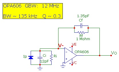
A typical amplifier is shown below. Ci is the total capacitance at the inverting input, including photodiode and op-amp contributions. Ri is the total input resistance at the inverting input
which is the parallel combination of the shunt resistance of the photodiode and the input resistance of the op-amp. Rf is the gain-setting feedback resistance and Cf is the total feedback
shunt capacitance, including stray capacitance in the feedback path. Ip is the photocurrent of the photodiode which for AC analysis will consist of a DC value with a superimposed AC component:
The complex transimpedance transfer function Tz(f) = Vo(f)/Ip of the transimpedance amplifier is:

where Zf is the parallel impedance of Cf and Rf and β(f) is the complex frequency-dependent feedback fraction
which is the same as the inverse of the noise gain NG(f). Ao(f) is the complex (including amplitude and phase) frequency-dependent open loop gain of the op-amp.
In this expression for Tz(f), Ao(f) is fully general and applies to any amplitude and phase for the open loop gain profile at any frequency. In the analysis here, it is always assumed that the circuit, including the op-amp, is operating in its
linear regime (i.e. not slew-rate limited, not current limited etc.) so that complex impedances at frequency f are meaningful. All circuit voltages and currents are therefore complex phasors
at frequency f and impedances, including Tz(f) are also complex. Often, only the magnitude of responses are plotted, for example |Tz(f)|.
Using superposition, the total circuit response is then the sum of responses from DC and all AC components of Ip.
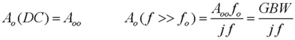
For the simple case of an open-loop gain profile with a single low frequency pole, the expression for Ao(f) is:

where Aoo is the DC open loop gain, typically 100 db (100,000) or higher and fo is the op-amp corner (pole) frequency, typically 10 - 50Hz. For this simple form of Ao(f),
the op-amp GBW product is simply Aoo x fo. For the sake of the analysis here, we will assume this simple form for the open-loop gain profile. (However, the open loop gain profiles
for real op-amps are often shaped by extra poles, particularly near the unity-gain frequency). For frequencies much less than fo (essentially DC) and much greater than fo, the open-loop
gain become:
Notice that the open-loop gain for f>>fo has a magnitude of GBW/f and a constant phase shift of -90°, simply the full accumulated phase shift of the single low frequency pole.
In a voltage feedback amplifier, an error voltage develops between the inverting and non-inverting terminals of the op-amp.
For an ideal op-amp with infinite open loop gain, this error voltage would be zero which would be a perfect "virtual ground".
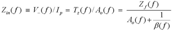
At any frequency, the effective complex input impedance (or "error impedance") at the non-inverting input
for this circuit configuration is the error voltage divided by the current Ip (with Ip defined as positive flowing into the inverting input node):
Depending on the components Ri, Ci, Rf, Cf, the input impedance will be reactive.
Any real op-amp has a finite open-loop gain which through negative feedback leads to the finite error voltage across the input terminals.
From the definition of open-loop gain, the input error voltage is the frequency dependent output voltage divided by the open-loop gain at that frequency.
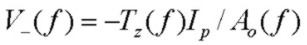
For the circuit above the error voltage is simply V-
the voltage at the inverting input relative to the non-inverting grounded input. Therefore the complex error voltage at any frequency is given by:

At DC, V- is extremely low due to the high DC open loop gain Aoo. At DC, the error voltage is just the DC output voltage RfxIp divided by the DC open-loop gain:

Note that the DC error voltage is opposite in sign to that of the output voltage, i.e. it is shifted -180° in phase relative to the output voltage.
Since the open-loop op-amp gain magnitude depends strongly on frequency, typically dropping at 20db/decade beyond fo,
the input offset voltage error magnitude will increase with frequency, causing the op-amp circuit to appear more non-ideal as the frequency increases. At frequencies much higher than fo,
the magnitude of the input error voltage is:

where Gain(f) = GBW/f is simply the amount of open-loop gain available at frequency f. Also, since the phase angle of Ao(f>>fo) is -90°, the phase shift of
the error voltage relative to the output voltage is (-180 + 90) = -90° and independent of frequency in the region f>>fo.
Note that given the output voltage, it is not necessary to know the detailed circuit component values to determine the error voltage.
If the feedback impedance is resistive (Zf = Rf) , the input impedance in this region up to the bandwidth limit is easily seen to be inductive:
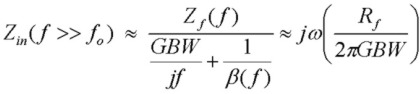
and for even higher frequencies where the op-amp gain GBW/f is lower than the noise gain 1/β(f), the input impedance becomes Z(f)β(f) or simply Zf||Zi as expected.
For a given magnitude of output voltage (obviously depending on Ip, Rf and f) and op-amp GBW product,
the input error voltage is easy to calculate. For example, with an op-amp having a DC open-loop gain of 100,000 and a GBW product of 20 MHz, for an output voltage of 3V,
the DC error voltage is 30 µV, but at a frequency of 1 MHz (where the amount of available open-loop gain is only 20), the magnitude of the error voltage is 150 mV.
Error Voltage and Photodiodes:
This error voltage for photodiode amplifiers may be important, particularly for photodiodes which are not reverse-biased since the error voltage represents a voltage drop across the photodiode which, if large enough,
will cause a nonlinear response as a function of incident optical intensity. (this effect is minimized if reverse-bias is applied to the photodiode). This will be clearly
important in analog circuits operating at higher frequencies. Note that the photocurrent Ip is always a reverse current. However the resultant error voltage will in general swing the photodiode
into slight forward or reverse bias (or if reverse bias is explicitly applied, the error voltage will be modulated slightly about the nominal reverse bias voltage value). This is true because the DC component of the
optical signal leads to a very small error voltage. However a superimposed AC component of Ip at a higher frequency contributes a much larger AC error term which causes the error voltage to swing above and below
ground, offset slightly by the DC error. However the output voltage level will be unipolar and positive.
In the configuration shown above, with the photodiode cathode (-) connected to the inverting input, DC photocurrent flows "downwards" from the anode to ground.
Since the current must be sourced by the op-amp output, current flows from the op-amp output through Rf toward the inverting input meaning that the
output DC voltage resulting from the photocurrent for this geometry is a POSITIVE voltage.
Comparison With Simulator Results:
To check the accuracy of the expressions above which assumed a fairly basic single-pole open-loop gain profile but an otherwise ideal op-amp, a circuit simulator was run showing the time response for the basic transimpedance circuit.
The photocurrent source was modeled as a DC offset current of 2 µA with a superimposed 1 µA AC component at 50 kHz. With a 1 Mohm Rf value, this leads to an output DC voltage
of 2.0 V with an AC component with amplitude of 1.0 V within the passband of the response. This would correspond to a received DC optical source with a 50% modulation signal at 50kHz.
The op-amp has a GBW product of 8 MHz. At the simulation frequency of 50kHz, the available open-loop gain is 160. The expected error voltage for the 50 kHz component
at the inverting input from the analysis above is expected to be Vo(50kHz)/160 and shifted by -90° relative to Vo(t).
Since the OP27 has a DC open loop gain of 1.8e6, the expected DC error voltage at the inverting input from the analysis above is expected to be Vo(DC)/1.8e6 or ~ 1µV.
The transient simulation below shows the Vo(t)
in the upper curve, and V- in the lower curve, labeled as V(1). The Vo voltage amplitude for the AC component is 0.94V. (This is slightly less than the passband value of 1.0V since the frequency
is approaching the 140 kHz 3db bandwidth of the transimpedance circuit). Therefore the expected error voltage based on the analysis
above is 5.9 mV. The error voltage amplitude from the simulation is 5.9 mV in agreement with the analysis above. Note also that the phase shift of V- relative to Vo is -90° as expected and
that V- has virtually no DC offset as expected:

The Error Impedance (Input Impedance of the Tz circuit):
As demonstrated above, it is easy to calculate the error voltage at any frequency using the simple expressions above for any given output voltage. However it is instructive to consider the error voltage in terms of
the transimpedance function Tz(f) and the photocurrent magnitude Ip = Ip(f). This is clearly equivalent to the approach above since the output voltage is Tz(f) x Ip.
This leads to a concept called the "error impedance" which is the input impedance of the transimpedance circuit configuration.
Using the definition of transimpedance Tz(f), the error voltage can be written as:
We will define a quantity ZV- called error impedance as follows:

This quantity is simply the frequency dependent input impedance or the V- input error voltage divided by the photocurrent Ip in Ohms (for example, µV (offset) / µV (photocurrent)
To demonstrate in more detail how the input error voltage changes with frequency, the first graph below shows the response functions for the circuit shown above with the values given. The magnitude of the
error impedance or input impedance is also shown, demonstrating a dramatic rise in error voltage as the frequency increases (the value plotted is actually 20*Log10(|ZV-|).
As mentioned above, this is the region in which the input impedance is inductive in character, increasing linearly with frequency or 20dB/decade. The rolloff of the error impedance at higher frequency corresponds to an input
impedance of Zi||Zf as mentioned above and for the circuit here, corresponds to a capacitive reactance due to (Cf + Ci) with an associated 20dB/decade decrease at high frequency:

The corresponding linear plot of the error impedance is shown below. For example since the DC error impedance is ~ 3.3ohm (Rf = 1Mohm divided by Aoo ~ 300,000), 1 µA of photocurrent will cause an error voltage of 3.3 µV.
However, at 50 kHz, the error impedance is ~ 4000 ohm, meaning a 4mV AC error voltage for each
µA of photocurrent and is double this value at the transimpedance f3db frequency of 135 kHz. Given the same op-amp, a transimpedance circuit with a much lower value of Rf, designed to be used
at higher frequency, would have a considerably higher error voltage, simply because the amount of open-loop gain is lower at higher frequency.
The value of the error voltage obviously scales with photocurrent Ip:

References