Transimpedance Cumulative Output Noise Voltage
Aug 26, 2012
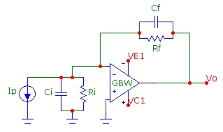
This cumulative output noise voltage calculation discussed here applies to this
transimpedance circuit:

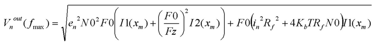
The general form for the total integrated output noise voltage or cumulative noise up to frequency fmax for the transimpedance circuit is given by:
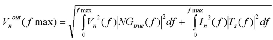
where Vn^2 is the sum of all the squared input voltage noise spectral densities that are amplified by the full noise-gain (equivalent noise sources at the NON-inverting input) and In^2 is the sum of all the squared equivalent input current-noise
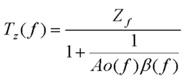
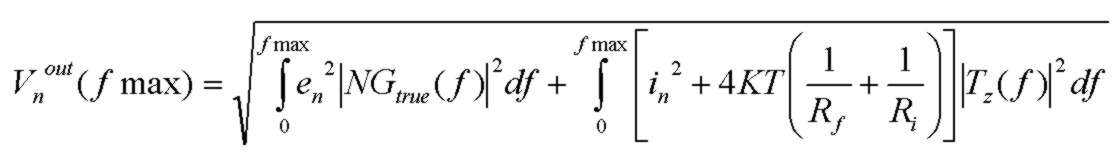
densities at the INVERTING-input. NGtrue(f) is the full noise-gain expression including the op-amp roll-off factor and Tz(f) is the full transimpedance transfer function:
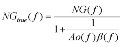
where the usual noise-gain expression is
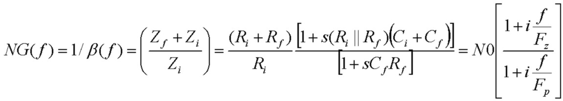
where Fz and Fp are the zero and pole frequencies of the noise gain:


Zf and Zi are the impedances of the feedback path (Rf || Cf) and the inverting input (Ri || Ci) respectively
and N0 is the DC noise gain (1 + Rf/Ri)
For the specific circuit shown, the total output voltage noise becomes:
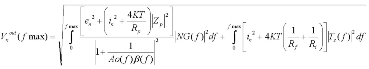
where en and in are the op-amp voltage noise and current noise densities and Zp is the impedance at the non-inverting input (Rp || Cp):

Note that the thermal noise contributions from Rf and Ri act essentially like current sources, generating output voltage by the full transimpedance transfer function (exactly the
same as the signal current Ip).
Simplifications
Using real frequency-dependent expressions for the op-amp voltage and current noise densities, the above expression could be numerically integrated to get accurate noise results.
Here, we will assume that the voltage and current densities en and in are constant in frequency (therefore ignoring low frequency 1/F noise etc..).
Also, although Rp is typically used for offset bias current cancellation, this is usually used with Cp to achieve a low-pass noise filtering effect in the transimpedance circuit (Zp).
Here, it will be assumed that the non-inverting input is grounded (Rp -> ∞ Cp -> 0) to simplify the analysis (although the integration with this noise source is not difficult).
With these simplifications, the circuit becomes:
and the total integrated output noise voltage or cumulative noise up to frequency fmax for the transimpedance circuit is given by:
For comparison with standard 2nd order transfer function form, it is useful to write the above result in this equivalent form:
GBW is the op-amp gain-bandwidth product (assuming a single-pole model for the open-loop gain),
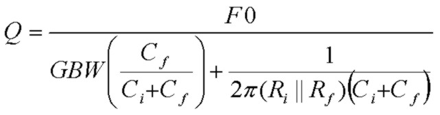
F0 is the natural resonant frequency of the transimpedance transfer function and N0 is the DC noise gain:
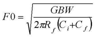
where Ci is the total input capacitance shunting the inverting input to ground, Cf is the total shunt capacitance across Rf and I1 and I2 are
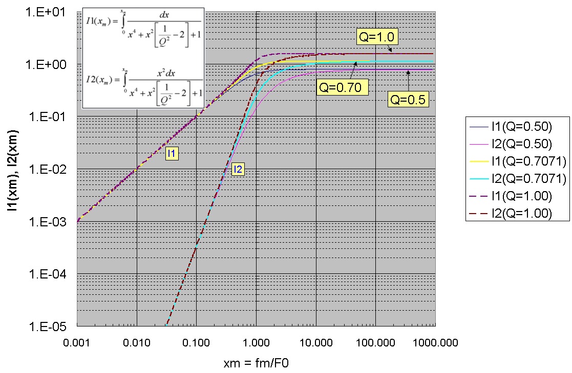
integrals which depend on Q and which describe the effect of the finite integration bandwidth.
Note that the integral I2(xm) reflects the effect of the noise-gain peaking on the noise contribution from op-amp voltage noise, and this effect scales with
the square of F0/Fz clearly showing the important effect of the noise-gain zero. The lower Fz, the greater the effect of noise-gain peaking.
The integrals for the cumulative noise voltage calculation are:


where the parameter x and its range xm are related to the resonant frequency and the frequency range fmax by:

and Q is the quality factor parameter describing the resonance of the transfer function:
The integrals I1 and I2 have exact analytical solutions which are plotted below for the 3 cases of most interest:
- Q = 0.50 (critically dampled)
- Q = 0.7071 (maximally flat response)
- Q = 1.00 (common design target but with 45 deg. phase margin and more overshoot and peaking)
The maximally flat case with Q = 1/√2 provides a very good compromise with good bandwidth, very good stability and flat transimpedance
frequency response with very small pulse overshoot. For the maximally flat case, the transimpedance 3dB bandwidth is exactly equal to the
natural resonant frequency: f3db = F0.
The total output voltage noise is obtained by integrating out to infinite frequency or xm --> ∞ . The total output noise can be
interpreted as an output maximum noise spectral density value times a "brick wall" noise bandwidth value.
Limiting cases are:
- xm >> 1 I1 = I2 --> Q π/2 (full noise integration out to infinite frequency)
- xm << 1 I1 --> xm I2 --> xm^3/3 (low frequency range)
where xm is fm/F0 and fm is the frequency limit for integration.
Calculating The Cumulative and Total Noise
The calculator below can be used to compute the total (integrated over all frequency) and the cumulative (up to frequency fmax) output noise voltage. The noise sources
include op-amp voltage and current noise sources, thermal noise sources and photodiode signal current and dark current shot noise sources. The calculation
for both the total and cumulative noise integrates over the exact transfer function of the circuit, thereby taking into account the second-order nature of the response.
The steps are:
- Enter the circuit data in the first section (note units) and click Get Params & Noise which shows each noise component and the total along with other parameters
- S/N is the signal to noise ratio for the specified optical power Psig
- In the lower section, enter the fmax value (in MHz) to determine the cumulative output voltage noise up to this frequency
- Click Get Cumulative Noise which uses ALL the data in the upper section of the calculator
- The parameters xm, F0, I1(xm) and I2(xm) and the cumulative noise components and total cumulative noise up to fmax are calculated and displayed
Note that clicking Get Params & Noise does NOT update the data in the Cumulative Noise section of the calculator.
If only TOTAL noise up to infinite frequency is required, the upper section of the calculator can be used independently of the lower section.
For convenience, 3 special buttons are provided which automatically calculate the required exact Cf value (given GBW, Rf, Ri and Ci) and all
other parameters in the upper section of the calculator for the 3 useful cases of:
- Q = 0.50 the critically damped case; no peaking in frequency response and no overshoot in pulse response
- Q = 1/√2 the maximally flat case; maximally flat frequency repsonse with 4% overshoot in pulse response
- Q = 1.00 the "45deg PM" case; 15% peaking in frequency response with 16% overshoot in pulse response
The calculator is also available separately and also with a minimal interface.
Note on Special Conditions:
Depending on the component values of Rf, Ci and GBW,
a solution for Cf
for underdamped responses, such as the maximally flat condition Q=1/√2 or the popular Q=1.0 case may not be possible.
This may occur for small values of Rf or Ci or GBW. (However, a Cf solution for the critically damped case Q = 0.5 will always be possible).
For the "maximally flat" case with Q = 1/√2, a Cf solution will only be possible under this condition:

For the common case with Q = 1.0, a Cf solution will only be possible under this condition:
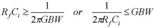
In both cases, this means that the zero frequency of the noise gain (or equivalently the pole frequency of the feedback factor β(f)) must be comparable to or less the op-amp GBW for a
Cf solutions with these Q values to exist. This condition will NOT be satisfied if the zero and pole frequencies of the noise-gain are considerably higher than the op-amp GBW.
In that case, the transimpedance f3db bandwidth will simply be controlled by the op-amp open-loop rolloff and f3db will be comparable to the op-amp GBW. Under this condition,
the circuit will typically have a Q value < 0.5 with Cf set to zero (or some nominally small stray value such as 0.3 pF)
and there will be negligible noise-gain peaking in the pass-band of the transimpedance response.
The circuit will have considerable phase margin and will be stable so that no compensation capacitance Cf will be required. Of course Cf could be added to reduce f3db and total
output noise.
Calculator Parameters
- GBW op-amp gain-bandwidth product
- en op-amp noise voltage spectral density
- in op-amp noise current spectral density
- Rf feedback resistance
- Ri total shunt resistance at inverting-input to ground
- Cf feedback shunt capacitance
- Ci total capacitance at inverting-input to ground
- Resp photodiode responsivity in A/W
- Id photodiode dark current
- Psig optical power received by photodiode
- Q quality factor of transimpedance transfer function
- Fz zero frequency of noise-gain function
- Fp pole frequency of noise-gain function
- F0 natural resonant frequency of transimpedance transfer function
- f3db 3 dB bandwidth of transimpedance transfer function
- NBWen effective "noise bandwidth" for en contribution
- NBWin_th effective "noise bandwidth" for Rf thermal or in contribution
- Ven total output noise voltage from en contribution
- Vth total output noise voltage from Rf thermal contribution
- Vin total output noise voltage from in contribution
- VId total output noise voltage from photodiode dark current Id contribution
- VPsig total output noise voltage from photocurrent signal shot noise contribution
- Vtotal total output noise voltage of all contributions (rms summed)
- S/N signal to noise ratio (at optical power level Psig) in dB
- fmax maximum frequency for cumulative noise voltage
- xm parameter for I1, I2 integrals xm = fmax/F0
- I1(xm,Q), I2(xm,Q) cumulative noise integrals
- VenC cumulative output noise voltage from en contribution up to fmax
- VthC cumulative output noise voltage from Rf thermal contribution up to fmax
- VinC cumulative output noise voltage from in contribution up to fmax
- VIdC cumulative output noise voltage from photodiode dark current Id contribution up to fmax
- VPsigC cumulative output noise voltage from photocurrent shot noise contribution up to fmax
- VtotalC cumulative output noise voltage of all contributions (rms summed) up to fmax
The Noise Bandwidth
When total noise integrated over all frequency is of interest (as opposed to cumulative noise up to a finite frequency limit), the noise bandwidth concept is useful.
The noise bandwidth is a "brick wall" filter bandwidth number which, when multiplied by the low frequency output spectral noise power density
of the noise generating source gives the same total power as that obtained by integrating the noise power density of the exact transfer function over all frequency.
Noise bandwidth NBW is a frequency and is defined via:
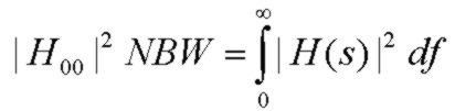
where H(s) is the voltage gain transfer function and Hoo is the low-frequency (usually maximum) value of the voltage gain transfer function. The corresponding value of the output voltage noise
is:
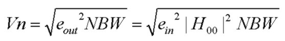
where eout is the output referred voltage noise spectral density and ein is the input referred voltage noise spectral density for the contributing noise source.
Both expressions are equivalent.
Clearly the concept of a noise-bandwidth is meaningful only when the spectral noise-density of the contributing noise component is independent of frequency. Also, transfer functions with gain
profiles that increase with frequency (for example the transfer function for the op-amp voltage noise contribution) are characterized by a noise-bandwidth number that is artifically large.
This arises because of the way noise-bandwidth is defined. However, even under these conditions, the noise-bandwidth
will correctly predict the total output noise since it is fundamentally derived from the exact integration of the true transfer function.
(1) Noise-Bandwidth: Simple RC Filter Case
As an elementary example, consider the total integrated thermal noise at the output of the simple RC filter below:
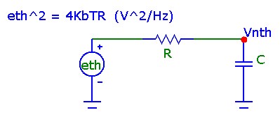
eth is the thermal noise voltage spectral density and vnth is the total output thermal noise voltage. The transfer function and half power (3db) frequency for this simple single-pole filter are:

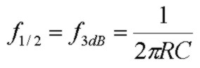
Simple integration over frequency provides the noise bandwidth for this filter as:

and the resultant total output thermal noise voltage is:
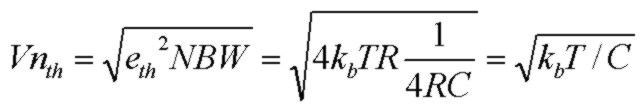
which is independent of the resistor R that sources the noise. This may seem surprising at first inspection, but is a simple consequence of higher R values creating proprotionally
higher thermal noise spectral power density. The RC filter action on the other hand receives a proportionally lower cutoff frequency. The two dependencies cancel out to yield a constant total output noise which
only depends on temperature and the filter capacitor value. Since the noise-bandwidth (or f3db bandwidth) grows larger as R becomes smaller, this implies usage of this total noise figure
requires that the overall bandwidth of the system must be significantly larger (> 20x) than the noise-bandwidth for the total noise value to be reasonably accurate. For system bandwidths lower than this,
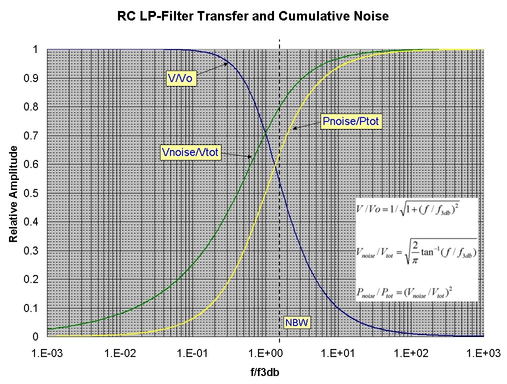
the graph below shows the voltage transfer function, cumulative output noise voltage and cumulative noise power at the output of an RC filter. The noise-bandwidth value is marked by a vertical dashed line:
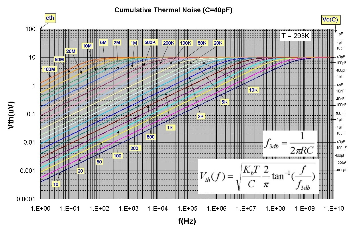
More specifically, the detailed graph below shows the cumulative thermal noise voltage (total thermal noise up to frequency f) in μV at T=293K (20C) across a fixed capacitor of 40 pF for the RC circuit.
Each curve corresponds to a different resistance value from 10 ohm to 100 Mohm as marked in the boxes.
These curves show clearly that the total thermal noise, integrated over ALL frequency, well past the f3db cutoff frequency for any RC combination
is the same for any resistance value. For a given R value, that common asymptotic value is approached near the corresponding f3db frequency for that RC combination.
For C=40pF, the total thermal noise voltage summed over all frequency is 10 μV. That asymptotic value depends on C and was given above as Sqrt(KbT/C), independent of R.
For different values of C, the curves for different values of R will be unchanged at lower frequencies, but will asymptotically approach a different value in proportion to Sqrt(1/C).
The scale on the right side of the graph shows the asymptotic value Vo(C) reached for different values of C.
For example, with Cf = 1000pF (1nF), the total thermal noise asymptotic value will be 2 μV, simply demonstrating the stronger thermal noise filtering action with a higher value of C.
Of course, since different resistor values have different (constant) thermal noise spectral density values of Sqrt(4KbTR), at low frequencies where the capacitor doesn't provide significant shunting,
the noise curves will be different with higher R values contributing greater thermal noise. In this low frequency region, the cumulative thermal noise voltage up to frequency f simply reduces to the familiar
result Sqrt(4KbTRf). In this low frequency range, the log-log plot shows a slope of 1/2 as expected for this dependency. The thermal noise voltage spectral density (noise per unit bandwidth) is
Sqrt(4KbTR) which is simply the value of the curves at 1 Hz (the left intercept).
For example, for R=50ohm, the thermal noise voltage spectral density is 0.9nV/√Hz .
The f3db values for each R for this set of curves with C=40pF is simply the intersection of a horizontal line at 7.07uV with each curve.
The corresponding noise-bandwidth value is 1.57f3db as was shown above:
(2) Noise-Bandwidth: Transimpedance 2nd Order Filter Case
The transimpedance circuit discussed above is described by a 2nd order transfer function and therefore the noise integration will be more complicated than the 1st order RC filter above.
The transfer function response is contained in the expressions involving I1, I2 integrals. Both I1 and I2 integrate
over infinite frequency to π/2Q. Examination of the general transimpedance noise expressions above
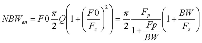
and substituting the values of Q and F0 shows that the noise-bandwidth for thermal Rf, Ri and in noise sources are identical and is given by:

where BW is the usual basic bandwidth derived from the DC closed-loop gain and the gain-bandwidth product of the op-amp and N0 is the DC noise-gain:

Notice that this noise-bandwidth term is independent of Ci.
Similarly the noise-bandwidth expression for the op-amp voltage noise contributor is:
Finally the total output voltage noise over all frequency, written in terms of the component noise-bandwidth factors is:
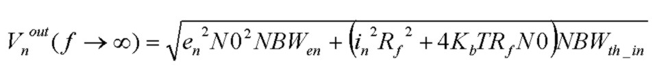
where the factors multiplying the noise-bandwidths are the output-referred spectral power densities at low frequency for each source, or equivalently, input-referred spectral power densities multiplied by the DC noise-gain squared.
For transimpedance circuits, usually Ri>>Rf and therefore N0 ~ 1. Also, as is often the case, if Fz<< GBW and Fp<< GBW, the noise-bandwidth expressions simplify to:


In this approximation, the thermal and in noise terms have a noise-bandwidth equivalent to a single-pole filter with a cutoff frequency at the
feedback pole frequency Fp, a satisfying result. Also, in this approximation notice that the noise-bandwidth for the op-amp voltage noise contribution is much larger, by a factor of GBW/Fz,
than the thermal and in noise-bandwidth. This is due to the significant gain peaking in the frequency-dependent noise-gain profile arising from the zero
due to Rf and Ci. In obtaining the total output noise, integration over the non-uniform noise-gain profile translates into an effective high noise-bandwidth for the en contribution.
Finally, in this approximation, the thermal noise contribution due to Rf simplifies to KbT/Cf, dependent only on the feedback shunt capacitance, independent of Rf and Ci.
This result is very similar to the result stated above for the simple RC filter example.
The Cumulative Noise Integrals I1, I2
 v
v
Since for the maximally flat case of Q = 1/√2, f3db = F0, setting the noise frequency integration limit to fm = f3db corresponds to xm = 1.
The log-log plots below show the linear and 3rd power dependence for I1 and I2 respectively for xm<<1: