
The Noise Gain
May 16, 2012
The feedback properties of an op-amp circuit determine the circuit stability. In the simplest scenario, a fraction β of the output signal is
passed back to the inverting (INV) input using a voltage divider network as shown in the two circuits below, the non-inverting NI voltage amplifier circuit,
and the current-to-voltage transimpedance TZ circuit. In general, the voltage divider network will consist
of complex impedances meaning that the feedback signal will be shifted in phase. Both circuits below have the same feedback fraction:


Assuming that the op-amp input impedance at the INV input is extremely high and no current is draw by the INV input, the voltage feedback fraction β at the INV input is:

The Noise Gain function is defined as the inverse of β:

It is called the noise gain because it is the dominant part of the voltage gain experienced by the op-amp input voltage noise and is identical
to the signal voltage gain of the non-inverting amplifier shown above. The noise gain will vary with frequency since Zf and Zi are in general complex impedances.
Basic network node analysis for the NI circuit shows the amplifier voltage gain transfer function
is given by:
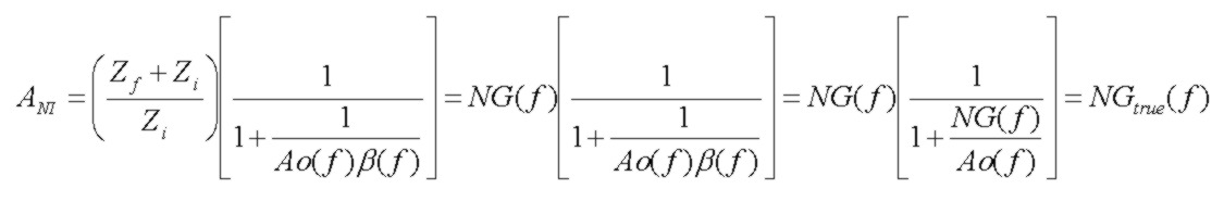
Note that the noise gain factor NG(f) doesn't represent the entire gain expression. It corresponds to the noise gain for an ideal op-amp with infinite GBW product. The second factor, sometimes
called the
error factor accounts for the finite (non-ideal) GWB product of an op-amp. The entire gain expression is sometimes called the True Noise Gain.
The essence of feedback loop stability is contained in the loop gain expression Ao(f)β(f) or equivalently Ao(f)/NG(f) where Ao(f) is the op-amp open loop gain response, which for a simple single-pole response is:

The frequency at which the magnitude of Ao(f)/NG(f) is unity (or equivalently the point at which the magnitude curves of Ao(f) and NG(f) intersect) must have a phase angle of less than 180 deg to ensure that
the feedback signal doesn't contribute to positive feedback and oscillation. Typically 45 degrees or more of phase margin (180 -Phase(Ao(f)/NG(f)) at the intersection point is adequate. Equivalently
this means that the magnitude curves on a log-log scale must have a rate of closure (net slope of intersection) of no greater than about 20 db/decade, the rate of slope for a single pole response.
Note that Ao(f) already contributes ~ 90deg of phase shift (fo ~ 10 Hz typically and f>>fo usually) so an additional pole in the feedback network will definitely drive the feedback into instability.
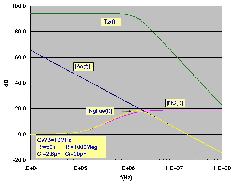
A log-log plot of the noise gain magnitude |NG(f)| and |Ao(f)| provides quick visual graphic insight into circuit stability. This applies to other op-amp
circuit configurations as well. For example, exactly the same error factor with identical stability criteria applies to the transimpedance circuit:

Note that in the case of the transimpedance transfer function, the ideal (infinite GBW op-amp) transimpedance reduces to simply Zf, independent of any Zi input impedance.
Examples
The examples below show Bode plots of Ao(f), NG(f) and NGtrue(f) for a typical noninverting amplifier and a transimpedance amplifier.
The only difference in the circuits is the value of Rf. Component values used in the simulation are shown. For the noninverting amplifier, the NGtrue(f) is the signal voltage gain. The two examples
demonstrate circuits where the noise gain zero frequency is lower than the pole frequency (TZ example) and cases where the zero frequency is HIGHER than the pole frequency (NI amp example).
In the NI example the zero and pole frequencies are high enough (due to the low value of Ri) that they don't effect the circuit response significantly and NG(f) is flat up to the intersection
with the open-loop gain profile. Note that in the TZ example, NG(f) increases markedly well before the intersection frequency, an effect well known in transimpedance circuits which
contributes to enhanced noise amplification:
Noninverting Amplifier (NI) Example:

Transimpedance (TZ) Amplifier Example:
References