
Photocurrent Shot Noise
Oct 01, 2012
Introduction
Transimpedance (Tz) circuits based on voltage feedback op-amps are often used as photodiode preamplifiers. These circuits make efficient use of available bandwidth, have excellent
signal to noise properties, particularly for high gain (Rf) configurations, and are relatively simple to design.
The total output noise of a basic Tz circuit is an important parameter and will limit the minimum detectable optical power level and also the signal to noise ratio achievable at different
power levels. It is well known that photocurrent originates from separation of electron-hole pairs, created by absorbed photons, in the PN junction depletion-layer field of the photodiode.
Therefore the photocurrent will contribute shot noise in the same way as op-amp input bias current is the origin of the op-amp input current noise density. In addition, if the photodiode
is reverse biased, there will be a leakage current (or "dark" current) which also contributes shot noise.
The shot noise spectral density is:
 or in convenient units
where I is the sum of the DC or rms photocurrent and any reverse DC leakage current and q is the electronic charge 1.6E-19 Coulombs.
This photocurrent signal shot noise contributes to the total output voltage noise of the Tz circuit.
For the Tz circuit, the output voltage noise contribution from this shot noise current is the shot noise current density multiplied by the feedback resistance and
the overall "noise bandwidth" of the noise measurement system.
This note demonstrates an example of photocurrent shot noise and compares measurements on a simple Tz photodiode circuit with the
modeled shot noise,
demonstrating that signal shot noise can dominate the total noise. An example and measurements of a current source in the same circuit which does not contribute
shot noise is also demonstrated.
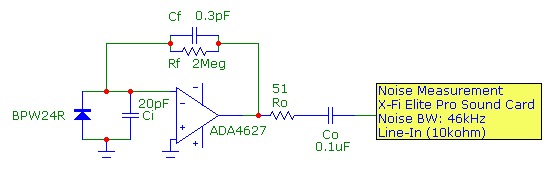
The Transimpedance Circuit:
The circuit used to demonstrate shot noise is shown below. The ADA4627 op-amp has a GBW product of 19 MHz, voltage noise spectral density en = 6nV/√Hz, current noise spectral density in = 2 fA/√Hz
which contributes negligible noise in this circuit and a total input capacitance of 15 pF. The BPW24R Si PIN photodiode was reverse biased at -6V giving a total input capacitance at the inverting input Ci of ~ 20pF. The
reverse leakage current of this photodiode was measured to be ~ 20pA at -6V reverse bias and therefore introduces negligible shot noise compared to the photocurrent shot noise.
A 2 MΩ feedback resistor was used. With only the stray feedback capacitance of ~ 0.3 pF, the circuit is stable. An output capacitor removes the DC output signal with a high-pass
corner of 160 Hz. The photocurrent DC level was determined my measuring the DC output voltage level before the output capacitor with a multimeter.
This circuit has a transimpedance f3db bandwidth of ~ 340 kHz:
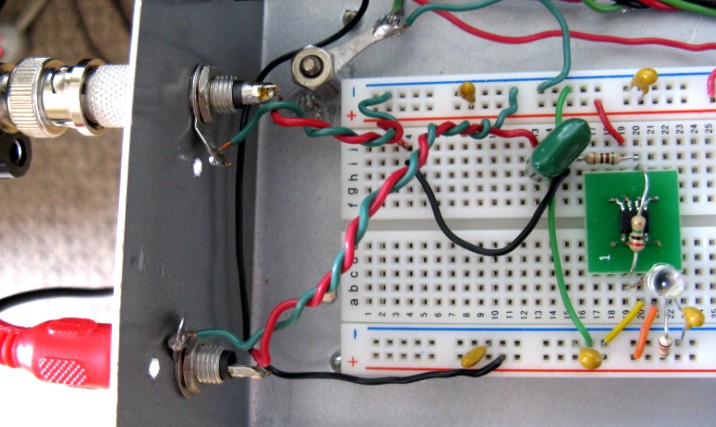
The protoboard, shown below, was housed in a shielded enclosure:
The Optical Source:
A TLDR490 650 nm red LED was biased at 10mA with a simple current source using a battery pack, independent of the dual power supply for the Tz circuit, was used for illumination.
The LED position was varied to change the illumination level and therefore the photocurrent generated by the photodiode.
A small hole in the top of the shielded Tz box was used for optical access as shown below (the LED faces down into the hole). Since we are only interested in the photocurrent value,
which can be determined from the measured output DC voltage, it is not necessary to know the responsivity of the photodiode at the wavelength of illumination.
During measurements, the entire assembly was covered with an opaque dark cloth. It was verified that the DC multimeter did not introduce extra noise into the measurement. The
op-amp offset output voltage is negligible compared to the values of output photovoltage used:

Noise Measurement Configuration:
To measure the noise, a low-noise audio sound card was used. The output of the Tz circuit was connected to the line-in of the sound card. A computer program analyzed the sampled
input analog waveform at 24bit/96kHz and calculated the rms noise voltage level. With the same cable connection from the shielded Tz circuit to the line-in, but shorted, the background
noise level was measured to be ~ 20 uV. The effective noise bandwidth of this sound card measurement circuit was determined to be ~ 46 kHz, about half the sampling frequency of 96kHz as expected.
Results:
Results of the measured output voltage, corresponding photocurrent (V/Rf), and the measured and
modeled noise in a 46 kHz noise bandwidth are shown below:
 Output DC Voltage          DC Photocurrent            Measured Noise       Modeled Noise
 -----------------          ----------------           ---------------      --------------
    0.40 mV                     0.20 nA                    44 uV                41 uV

    0.50 V                      0.25 uA                   134 uV               128 uV

    1.40 V                      0.70 uA                   220 uV               208 uV

    2.45 V                      1.22 uA                   285 uV               272 uV
With the photodiode well shielded from stray light with negligible photocurrent, the output rms noise voltage of 44 µV (corrected for the 20 µV background noise)
compares well with the modeled result of 41 µV, dominated by the thermal noise of Rf. (The output noise voltage remained at 44 µV with the photodiode removed).
The effect of the photocurrent shot noise is clearly seen in the increased noise measured at DC photocurrent levels above 0.1 uA corresponding to received optical power levels
above ~ 200 nW at this wavelength. The measured results are in good
agreement with the modeled results, and demonstrate how the photocurrent signal shot noise can dominate the total noise at higher optical illumination levels.
Shot Noise and Signal To Noise and Dynamic Range:
To demonstrate how important photocurrent signal shot noise is in this type of circuit, consider a circuit with a maximum output signal level of 2.45Vrms (equivalent to the highest DC level above for shot noise purposes).
For the noise bandwidth of 46kHz with an rms shot noise of 285 µV at this illumination level, the signal to noise ratio is 79 dB. However, if we neglect signal shot noise and assume the total noise is the total circuit noise of 44 uV,
we would (incorrectly) calculate a signal to noise ratio of 95 dB. This demonstrates very clearly that shot noise must be considered in photodiode amplifier circuits of this type.
The simulation chart below for the circuit above demonstrates how shot noise due to photocurrent (or any current source at the inverting input originating from PN junction current) contributes to the total output
voltage noise. The graph shows the output voltage noise contribution from each source (integrated over all frequency as compared to the restricted 46kHz noise bandwidth used above) and the total rms output voltage noise as a function of photocurrent
from 1 nA to 1 µA. Also shown is the SN ratio which, at low photocurrent increases linearly with photocurrent (or 20 dB per decade of photocurrent) since the photocurrent shot noise contribution to noise is negligible in this region.
In this region, the total output voltage noise is ~ 290 µV and is dominated by the op-amp voltage noise contribution of 270 µV
with a small contribution from the thermal noise due to Rf of 115 µV.
At higher photocurrent, where the shot noise of the photocurrent dominates the total output noise, the SN increases at the lower rate of 10dB per decade of photocurrent:

Current Source Without Shot Noise:
Not all current sources are associated with shot noise. For example DC current sourced by an ideal voltage source flowing through a resistance does not contribute shot noise.
Shot noise fundamentally arises from the random and independent generation or flow of carriers which occurs in junction carrier current flow and the photoelectric generation process.
However, the processes underlying ohmic conduction are dominated by carrier scattering processes which means that the flow of carriers is a correlated process leading to very
slow effective drift velocities in conductors.
A simple example of a current source which doesn't produce shot noise is a voltage source in series with a large resistance. Assuming an ideal voltage source, there is no shot noise but of course there is thermal noise.
To demonstrate this, consider the circuit below in which the photodiode has been replaced by voltage source Vi = 5.5VDC and a high resistance value Ri=10MΩ which represents
a current source of 0.55µA at the inverting input of the Tz amplifier. The actual circuit, which is an inverting amplifier configuration with signal voltage gain of -0.2,
and the Norton-equivalent circuit, which is a Tz configuration with current source Ii and finite Ri, are shown below.
If this current source produced shot noise, the corresponding output voltage noise would be 180 µV in a 46kHz noise bandwidth :
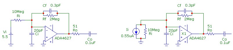
The measured output voltage noise in the 46kHz noise measurement bandwidth was 48 µV at the DC output voltage of 1.1VDC corresponding to 0.55µA.
From the simulation which includes the effect of Ri, the expected output voltage noise is 44 µV in good agreement
with the measured result and demonstrating that indeed this current source is not contributing shot noise. Finally we note that compared to the original photodiode circuit with a total output voltage
noise of 44 µV under dark conditions dominated by thermal noise of Rf, the higher value of 48 µV in this circuit is exactly what is expected for the increase in thermal noise
due to the introduction of Ri into the circuit, resulting in a DC noise gain of 1.2 which amplifies the thermal noise due to the parallel combination of Ri and Rf.
References