Transimpedance Amplifier with Butterworth PostAmp Filter
Jan 22, 2013
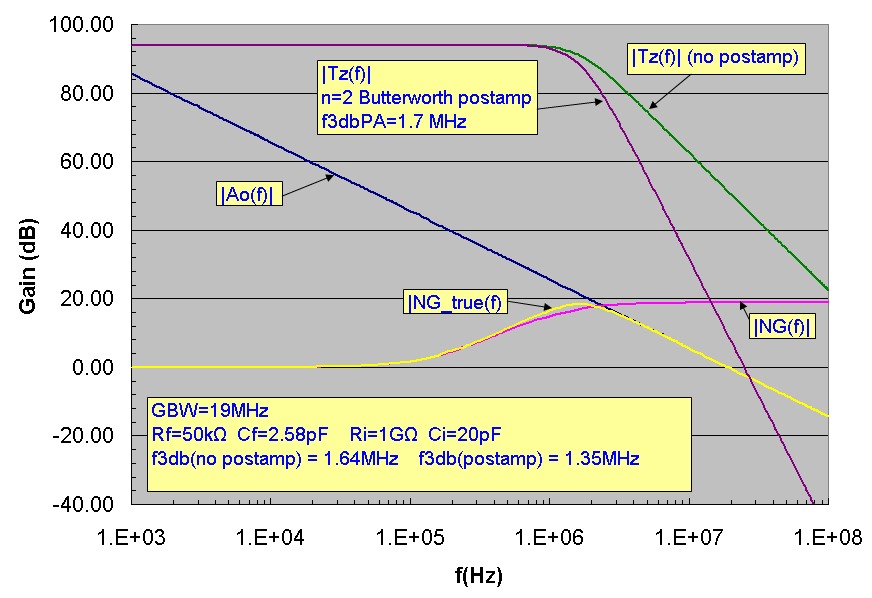
This note provides a simple example of the typical noise-reduction available when a transimpedance (Tz) amplifier is used with a tandem post amplifier filter. The example below
uses a 2nd order Butterworth filter with unity gain (at low frequency) as the post amplifier. The design f3db bandwidth of the Butterworth filter is 1.7MHz, slightly higher than
the f3db bandwidth of 1.64 MHz for the transimpedance amplifier alone. The transimpedance response curves show the gain of the transimpedance amplifier alone, and with the
Butterworth filter added. (The other curves in the response graph are for the transimpedance amplifier alone). The design of the transimpedance amplifier alone is approximately
the Q=1/√2 case (in fact a Butterworth design itself) corresponding to maximally flat frequency response. The response of the Tz amplifier alone shows the expected
40dB/decade drop off characteristic of a 2nd order response at high frequency.
WITH the Butterworth post-filter added, the final response at high frequency is 4th order with a rolloff of 80dB/decade. (Note that the combined response is not exactly a 4th order
Butterworth filter response) :
The graph below compares the cumulative noise for the Tz amplifier alone and with the 2nd order post amplifier added. The significant reduction of the noise contribution
due to the op-amp voltage noise source en is evident, with a reduced total output voltage noise ~ 3dB at the expense of a slight f3db reduction from 1.64MHz to 1.35 MHz.

The Butterworth post amplifier above was assumed noiseless. The achievable noise reduction will depend on the component values and op-amp used in the post-amplifier design. The results
above represent the best possible noise reduction. To estimate the noise contributed by the post-amplifier, consider a single op-amp Sallen-Key implemention of a 1.7MHz 2nd order Butterworth filter is shown below:

The GBW product of the op-amp should be at least ~ 5 x f3db of the filter design bandwidth, or about 10 MHz to ensure the step filter rolloff over a sufficient high-frequency range.
Since the design is a 2nd order Butterworth, it is easy to estimate the thermal noise contribution from resistor R1 of the filter circuit since it represents a flat noise voltage source
at the input to the filter. For 2nd order filters with Q=0.707, the noise bandwidth is 1.111xf3db or about 1.9MHz.
By comparison, the thermal noise contribution from R2 and the filter op-amp voltage noise en contribution require more careful scrutiny. Both these noise sources,
due to the filter feedback network, show some gain peaking about the nominal 0 dB response. In fact the noise contribution from en, apart from the peaking effect, is similar to a follower and
extends to the GBW product limit of the op-amp. Therefore the GBW product of the filter op-amp should be limited to avoid excessive en contributions to the total output voltage noise.
It is not difficult to calculate the transfer functions for noise sources at R2 and en in this circuit. Assuming for simplicity an ideal op-amp (infinite GBW product), the rather complex transfer
functions can be integrated over the entire frequency range. Assuming a cut-off frequency for noise integration (in this case) at 10 MHz and an op-amp en = 3nV/√Hz, the output
voltage noise contributions are thermal noise from R1 = 5.5 µV, thermal noise from R2 = 9.1 µV and op-amp voltage noise of 13.3 µV.
Comparing these additional output noise voltages to noise voltages at the output of the filter originating from the Tz amp along, it is obvious that the noise added by this Butterworth filter using
a 10 MHz GBW op-amp with fairly low en only increases the total output noise slightly (from 58 - 60 µV or 0.3dB). Intuitively, the thermal noise contribution of Rf in the Tz circuit dominates the overall thermal noise since Rf>>R1,
and the considerable voltage noise peaking in the Tz circuit swamps the voltage noise of the post filter op-amp even though the post-amp noise bandwidth extends to 10 MHz.
(Note that higher values of R1=R2 in the Butterworth circuit design would lead to higher thermal noise which would eventually cause the noise contribution of the post-amplifier to be significant).
Noise Expressions
Although it is possible to numerically compute the total noise output for any post-amplifier filter function shape, it is useful to have accurate closed-form expressions for quick computation for
a common target design scenario. For this purpose, the noise contribution from the post-amplifier filter will be ignored which can be a good approximation with properly selected post-amp components
as discussed above.
Consider the transimpedance circuit shown below with the low-pass 2nd order filter post amplifier:

Since a good design target with substantial phase margin is the Butterworth maximally flat response with Q=1/√2, we will
assume that both the transimpedance stage alone and the LP post 2nd order filter are separately designed with this same Butterworth Q value and the same f3db frequency.
For the transimpedance stage, this means selecting a proper value for the feedback capacitance Cf to target this Q value,
given the other component values and the op-amp GBW.
The LP filter stage could be a Sallen-Key filter stage with components chosen to obtain the same f3db and Q=1/√2 as the transimpedance stage.
The overall f3db of the combined stages is of course slightly smaller. It is easy to show by simple
inspection of the combined transfer function for the two 2nd order stages that the net bandwidth is f3db*√(√(√2 - 1))) or 0.8022*f3db (similar to the example provided above).
For this Butterworth case, it is easy to analytically integrate the combined transfer functions to obtain the
total integrated output voltage noise. These results are essentially a calculation of the total "noise bandwidth" of the combined circuit.
The results for the Tz stage alone and with both stages are:
For the 2nd order Tz stage alone:
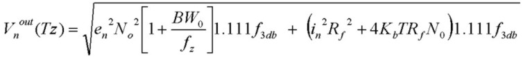
- The factor 1.111f3db is the noise bandwidth for the thermal and op-amp current noise contributions
- The extra factor BW0/fz for the op-amp voltage noise source, shows the strong effect of noise-gain peaking associated with input capacitance Ci and fz
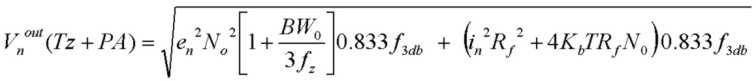
For the combined Tz and LP filter stages:
- The factor 0.833f3db for the noise bandwidth of the thermal and op-amp current noise contributions is lowered to exactly 75% of the value for the Tz stage alone
- The effect of BWo/fz is reduced to exactly 25% of the value for the Tz stage alone, indicating the potential benefit for noise reduction
For the thermal noise and op-amp current-noise components, the output voltage noise contributions will therefore be filtered to 87% of the value without the post-amp filter and the
output voltage noise originating from the en of the Tz op-amp stage will be filtered to 50% (or -3db) of the value without the post-amp filter, assuming that BW0/fz >> 1.
Since typically the en noise of the op-amp in transimpedance circuits will dominate the total noise, using this type of post-filter will have a substantial effect on total output noise reduction.
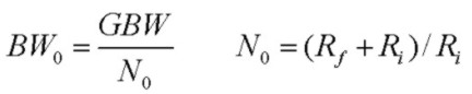
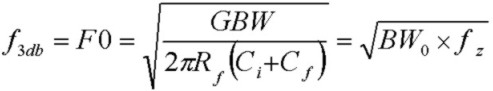
In the expressions above, N0 is the DC noise gain, BW0 is the nominal noise bandwidth, f3db is the 3db transimpedance bandwidth of the transimpedance (or post-amp
filter) stage alone FOR THE CASE OF Q=1/√2, and fz is the zero frequency of the transimpedance stage: