
Transimpedance Photodiode Amplifier: Bandwidth Study
Feb 07, 2013
This article demonstrates the dependency of photodiode transimpedance amplifier response bandwidth on the transimpedance gain. An intermediate speed low noise and low offset op-amp, the
AD8065 with a GBW=65MHz was used.
The gain in the passband of the basic transimpedance amplifier, a current-to-voltage converter, is set with the feedback resistor Rf. The response stability (phase margin) is set with the shunt capacitance Cf in parallel
with the feedback resistance. Efficient designs make effective use of the available op-amp GBW product with good phase margin. Simple design synthesis equations were used
in this study to target Q values from between 0.6 and 0.8 where Q is the "quality factor" of the circuit response. High values of Q (>1) are associated with circuits having significant peaking
in frequency response and large pulse overshoot. Low values of Q (<0.5) are heavily damped circuits which don't make efficient use of the op-amp GBW product. A good design point is Q=1/√(2) ~ 0.71 which
is the maximally flat "Butterworth" frequency response case with phase margin > 60°. This design guarantees excellent stability. For Q=1/√(2) the exact F3db frequency and required feedback
capacitance Cf are given by:

where Ci is the total capacitance at the inverting input of the op-amp to ground.
For this value of Q, F3db is identical to the circuits undamped natural resonant frequency. It is simply the geometric mean of GBW and the circuits "zero" frequency 1/2πRf(Cf+Ci) . In most cases of interest,
Ci >> Cf.
Note that the F3db value (for this design target) scales as √GBW, as 1/√Rf and as 1/√(Ci+Cf) . This facilitates easy predictions of response changes as GBW and Rf are varied.
For example, assuming Cf is chosen as above to target the Q=1/√(2) case, and assuming the same Rf and (Ci+Cf) values,
choosing an op-amp with GBW=1.5GHz instead of the 65MHz device used in this study will increase the F3db by a factor of 4.8. Note also that for very high GBW, less feedback shunt capacitance is required
and for large Rf values, the parasitic Cf value may limit the available transimpedance bandwidth.
Circuit Response Results:
The basic circuit schematic and measured impulse response for 3 circuits with different values of Rf/Cf are shown below. The op-amp was powered with a +/- 5V supply and measurements were performed
on a breadboard in a shielded box shown below. The BPW24R photodiode was biased at -5V with a response bandwidth of 25MHz. Noise measurements in the dark verified the expected behaviour based on the Rf value with this op-amp.
An infrared LED optical impulse with rise/fall times of ~ 20ns
was used as the source to measure the impulse response and is fast enough to not limit the impulse response measurements for the circuit bandwidths here. The optical source was positioned to achieve approximately
the same peak response amplitude of ~ 0.8Vpeak. The background noise floor is limited by the scope input at ~ 1mVrms for all 3 circuits. The circuit output offset voltage due to the op-amp is < 0.5mV in all cases.
A low bandwidth Digilent Analog Discovery scope
with an effective bandwidth of ~ 10MHz was used. The points in the data are the 100MSPS sampling points at intervals of 10 ns for this scope. :
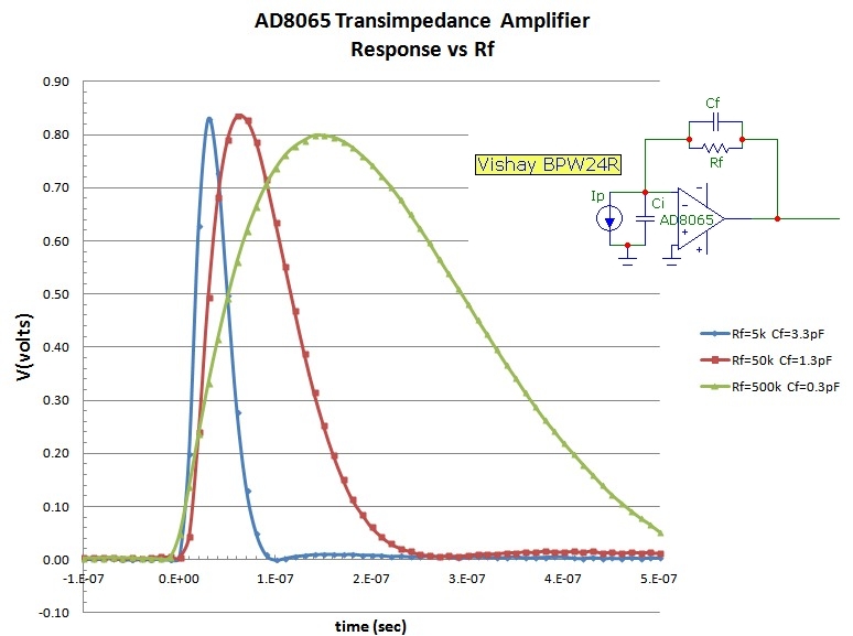
The -3db small-signal bandwidths for the 3 examples shown are 11 MHz, 3.3MHz and 1.5 MHz for Rf=5kΩ 50kΩ and 500kΩ respectively with the values of Cf shown. The Q values are between 0.60 and 0.80.
With a +/-5V supply, assuming a maximum output voltage of 4Vp (which means the 180V/µs slew-rate for this op-amp will start limiting the response at f ~ 7 MHz at this amplitude), the chart below shows,
for each of the circuits above,
the maximum photocurrent, the photocurrent value for an output voltage of 1mVrms (the noise floor of the Discovery scope) and the minimal detectable photocurrent Ip_NEP
(corresponding to the noise output of the transimpedance circuit). The last column shows the modelled total cumulative output voltage noise of the transimpedance amplifier up to 10 MHz.
The measurement dynamic range with this circuit, using the Discovery scope, is 72dB:
   Rf         Ip_max        Ip_1mVout       Ip_NEP         Vn_out (10MHz)
   --         ------        ---------       ------         --------------

   5 k        0.8 mA        0.2 uA          13 nA             65 uV

  50 k         80 uA         20 nA           4 nA            180 uV

 500 k          8 uA          2 nA         0.9 nA            440 uV
The amount of received optical power corresponding to these photocurrent levels is determined by the conversion efficiency or responsivity of the photodiode in A/W.
In the red and IR parts of the optical spectrum ( λ > 600nn) , typical responsivities are ~ 0.5A/W. Using this benchmark responsivity, the received optical powers are therefore
about twice the corresponding photocurrent values. For example the 50kΩ case with Ip_NEP = 4 nA corresponds to a minimal detectable received optical power of 8 nW.

The protoboard circuit above shows the components for the 5kΩ case. The parasitic capacitance across the feedback resistor is ~ 0.3 pF. The biasing network for the photodiode is at the lower
left (10kΩ series resistor with decoupling capacitor).