
Advanced Op-Amp Noise Calculator
Oct 03, 2012
This output noise voltage calculator for voltage-feedback op-amps applies to the
circuit shown below. Details of the theory, equations and approximations used in the calculator are provided elsewhere. It can be used to calculate f3db bandwidth and output noise for transimpedance, non-inverting and inverting amplifier configurations.
Parameter names are described below the calculator:

Calculating The Noise With The Calculator
The calculator above can be used to compute the total (integrated over all frequency) and the cumulative (up to frequency fmax) output noise voltage. The noise sources
include op-amp voltage and current noise sources, thermal noise sources and photodiode signal current and dark current shot noise sources for the tranimpedance circuit case.
The calculation for both the total and cumulative noise integrates over the exact transfer function of the circuit, thereby taking into account the second-order nature of the response.
The steps are:
- Enter the circuit data in the first section (note units) and click Get Params & Noise which shows each noise component and the total along with other parameters
- S/N is the signal to noise ratio for the specified optical power Psig
- In the lower section, enter the fmax value (in MHz) to determine the cumulative output voltage noise up to this frequency
- Click Get Cumulative Noise which uses ALL the data in the upper section of the calculator
- The parameters xm, F0, I1(xm) and I2(xm) and the cumulative noise components and total cumulative noise up to fmax are calculated and displayed
Note that clicking Get Params & Noise does NOT update the data in the Cumulative Noise section of the calculator.
If only TOTAL noise up to infinite frequency is required, the upper section of the calculator can be used independently of the lower section.
For convenience, 3 special buttons are provided which automatically calculate the required exact Cf value (given GBW, Rf, Ri and Ci) and all
other parameters in the upper section of the calculator for the 3 useful cases of:
- Q = 0.50 the critically damped case; no peaking in frequency response and no overshoot in pulse response
- Q = 1/√2 the maximally flat case; maximally flat frequency repsonse with 4% overshoot in pulse response
- Q = 1.00 the "45deg PM" case; 15% peaking in frequency response with 16% overshoot in pulse response
Note on Special Conditions:
Depending on the component values of Rf, Ci and GBW,
a solution for Cf
for underdamped responses, such as the maximally flat condition Q=1/√2 or the popular Q=1.0 case may not be possible.
This may occur for small values of Rf or Ci or GBW. (However, a Cf solution for the critically damped case Q = 0.5 will always be possible).
For the "maximally flat" case with Q = 1/√2, a Cf solution will only be possible under this condition:

For the common case with Q = 1.0, a Cf solution will only be possible under this condition:
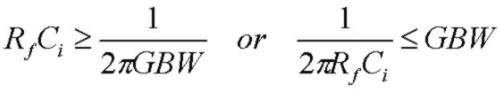
In both cases, this means that the zero frequency of the noise gain (or equivalently the pole frequency of the feedback factor β(f)) must be comparable to or less the op-amp GBW for a
Cf solutions with these Q values to exist. This condition will NOT be satisfied if the zero and pole frequencies of the noise-gain are considerably higher than the op-amp GBW.
In that case, the transimpedance f3db bandwidth will simply be controlled by the op-amp open-loop rolloff and f3db will be comparable to the op-amp GBW. Under this condition,
the circuit will typically have a Q value < 0.5 with Cf set to zero (or some nominally small stray value such as 0.3 pF)
and there will be negligible noise-gain peaking in the pass-band of the transimpedance response.
The circuit will have considerable phase margin and will be stable so that no compensation capacitance Cf will be required. Of course Cf could be added to reduce f3db and total
output noise.
Calculator Parameters
- GBW op-amp gain-bandwidth product
- T(°C) temperature in Celsius (for thermal noise)
- en op-amp noise voltage spectral density
- in op-amp noise current spectral density
- Rf feedback resistance
- Ri total shunt resistance at inverting-input to ground
- Cf feedback shunt capacitance
- Ci total capacitance at inverting-input to ground
- Resp photodiode responsivity in A/W
- Id photodiode dark current in nA
- Psig optical power received by photodiode in µW
- Q quality factor of transimpedance transfer function
- Fz zero frequency of noise-gain function
- Fp pole frequency of noise-gain function
- F0 natural undamped resonant frequency of transimpedance transfer function
- f3db -3 dB bandwidth of transimpedance transfer function
- f3db_NI -3 dB bandwidth of non-inverting amplifier (or true noise-gain) transfer function
- NBWen effective "noise bandwidth" for en contribution
- NBWin_th effective "noise bandwidth" for Rf thermal or in contribution
- Ven total output noise voltage from en contribution
- Vth total output noise voltage from Rf and Ri thermal contribution
- Vth_p total output noise voltage from Rp thermal contribution
- Vin total output noise voltage from in with Rf, Ri contribution
- Vin_p total output noise voltage from in with Rp contribution
- VId total output noise voltage from photodiode dark current Id contribution
- VPsig total output noise voltage from photocurrent signal shot noise contribution
- Vtotal total output noise voltage of all contributions (rms summed)
- S/N signal to noise ratio (at optical power level Psig) in dB
- fmax maximum frequency for cumulative noise voltage
- xm parameter for I1, I2 integrals xm = fmax/F0
- I1(xm,Q), I2(xm,Q) cumulative noise integrals
- VenC cumulative output noise voltage from en contribution up to fmax
- VthC cumulative output noise voltage from Rf and Ri thermal contribution up to fmax
- VthC_p cumulative output noise voltage from Rp thermal contribution up to fmax
- VinC cumulative output noise voltage from in with Rf, Ri contribution up to fmax
- VinC_p cumulative output noise voltage from in with Rp contribution up to fmax
- VIdC cumulative output noise voltage from photodiode dark current Id contribution up to fmax
- VPsigC cumulative output noise voltage from photocurrent shot noise contribution up to fmax
- VtotalC cumulative output noise voltage of all contributions (rms summed) up to fmax